A Simple Explanation on the Crystallization Kinetics of a CW Laser Crystallization of Amorphous Silicon
- PDF / 368,608 Bytes
- 6 Pages / 612 x 792 pts (letter) Page_size
- 79 Downloads / 446 Views
I2.3.1/A3.3.1
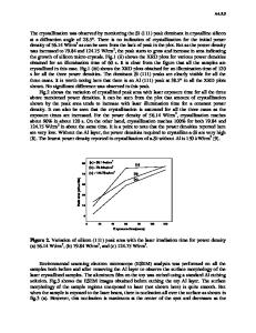
A SIMPLE EXPLANATION ON THE CRYSTALLIZATION KINETICS OF A CW LASER CRYSTALLIZATION OF AMORPHOUS SILICON Seong Jin Park, Sang Hoon Kang, Yu Mi Ku, and Jin Jang Advanced Display Research Center, Kyung Hee University, Seoul 130-701, Korea ABSTRACT We have studied a CW laser crystallization (CLC) of various-shaped a-Si patterns on glass with changing scanning speed and laser power. The crystallized region inside the patterns showed 3 distinct regions, which is distinguished by their grain size; fine grains of several tens of nanometers near the edge of the pattern, very large grains over a few micrometers at the center of the pattern, so called Sequential Lateral Crystallization region and large grains about a micrometer or less between SLC and fine grain regions. This phenomenon is due to the formation of 2-D temperature gradient inside the pattern. One is the temperature gradient between the edge and center; the temperature of outer region is lower than that of inner region during or right after a CW laser scanning. The other is the temperature gradient along the scan direction; the temperature of starting region of a CW laser scanned area is lower than that of ending region. The former contributes mainly to make molten silicon area inside a pattern, and the latter induces lateral growth along the scan direction to make long grains in SLC region. INTRODUCTION Recently, a CW laser crystallization of amorphous silicon (a-Si) using a DPSS laser, so called CLC, has been reported as an alternative method to get a high-quality poly-Si on glass substrate.[1-3] The a-Si is crystallized by the scanning of a CW laser and the large (long) grains are obtained along the laser scanning direction under adequate scanning speed and laser power. Not only the electric characteristics of CLC poly-Si TFT shows nearly the same as that of MOSFET on SOI wafer, but also CLC has several advantages such as simple, easy and low cost process compared to the conventional sequential lateral solidification (SLS) using an excimer laser.[4] Although there are some of papers regarding electrical and structural characteristics of CLC poly-Si, little has been known about the crystallization kinetics. In order to understand the crystallization mechanism of CLC, we have studied CLC of various-shaped a-Si patterns on glass with changing scanning speed and laser power. EXPERIMENTAL DETAILS The samples were prepared as follows. A silicon oxide (SiO2) layer of 400 nm was deposited on a glass (Corning 1737) prior to the deposition of an amorphous silicon (a-Si) layer. The thickness of the a-Si was 170 nm. We used a plasma enhanced chemical vapor deposition (PECVD) method to deposit SiO2 and a-Si layers. Dehydrogenation of the a-Si was done by a furnace annealing at 480 oC for 5 hrs. After that the a-Si layer was patterned with various shapes and sizes (rectangles, triangles and circles) by using a photolithographic process.
I2.3.2/A3.3.2
A 2ω CW (continuous wave) DPSS (diode pumped solid state) laser with the wavelength of 532 nm was used to c
Data Loading...