Thermal and Electromigration Effects on the Surface and Aluminum/Aluminum Oxide Interface of Aluminum Metallizations
- PDF / 2,511,967 Bytes
- 6 Pages / 414.72 x 648 pts Page_size
- 62 Downloads / 353 Views
GEORGE 0. RAMSEYER, JOSEPH V. BEASOCK, WILLIAM K. SYLLA AND LOIS H. WALSH Rome Laboratory/ERDR, 525 Brooks Rd., Griffiss AFB, NY 13441-4505
ABSTRACT Thermal and electromigration effects on the thicknesses of aluminum oxide at the aluminum-1% silicon/thermal silicon dioxide interface were quantitatively determined by AES. Void sites corresponded with thinner aluminum oxide thicknesses at this interface. Changes in surface topography and grain structure were quantitatively determined for thermally annealed aluminum-]% silicon metallizations by AFM. INTRODUCTION In 1965 Blech and Sello [1] first recognized thin film electromigration as a limiting factor in microelectronics reliability. Two years later Black [2] correlated electromigration induced failure times with conductor geometry and microstructure. Since then various combinations of passivation, alloying, composition, layering, and microstructure modifications have been used to control electromigration at micron dimensions[3]. Within the next few years metallization interconnects with nanometer dimensions will become the industry standard. The relative importance of the factors which effect electromigration and other stress induced failure mechanisms at these nanometer dimensions is not completely understood. Surface analysis techniques such as Auger Electron Spectroscopy (AES) provide elemental information from the top few atomic layers of solid materials. By profiling with an ion beam, solids can be characterized as a function of depth. The area characterized by this technique is of nanometer dimensions normal to the profiling direction. Small shifts in AES spectra are related to the chemistry at atomic dimensions, and these shifts are particularly pronounced for aluminum. Atomic Force Microscopy (AFM) allows quantitative characterizations of surface topography with atomic resolution. Previously the voids in 60 life tested meandering stripes were characterized [4]. More than 98% of the 1900 voids detected were located at the corners of the aluminum/thermally grown Si0 2 interface. It was also determined that for the meandering test structure the highest inplane tensile stress occurred at the middle of this interface [5], and that the highest out-of-plane stresses occur at the edges of this interface, The largest thermal gradient stresses also have been determined to occur at the edges of this interface [6]. Here we are presenting evidence of changes in the chemistry of this interface under thermal and electromigration stresses. 329 Mat. Res. Soc. Symp. Proc. Vol. 318. @1994 Materials Research Society
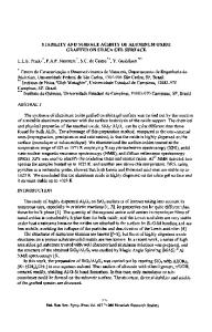
Fig. 1 Light microscope image of a meandering test structure. EXPERIMENTAL The width of each of three meandering test stripes was 3 pm, and the total length of each stripe was 1690 plm. These meandering test structures (Figure 1) were fabricated by sputter depositing 800 nm of Al-]% Si onto thermally annealed silicon wafers. The thickness of the thermally grown SiO 2 was 400 nm. The meandering test patterns were then etched into the aluminum film. A 800 nm passi
Data Loading...