Mechanisms of Stress-Induced and Electromigration-Induced Damage in Passivated Narrow Metallizations on Rigid Substrates
- PDF / 1,861,048 Bytes
- 9 Pages / 576 x 777.6 pts Page_size
- 61 Downloads / 389 Views
stresses in the metallization are concerned, is its coefficient of thermal expansion (CTE). Because CTE for the common ceramic passivation materials is much smaller than that for aluminum and is about that of silicon, we can assume to a fair approximation that the metal lines are embedded in a silicon matrix. A change of temperature from To to T induces thermal strains of e'i = e\ = eT3 = Aa(T - To),
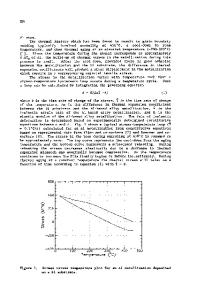
where Aa = aA]-as is the differential CTE. The thermal stresses can be found by multiplying the corresponding elastic strains by suitable moduli. Thermal stresses in passivated line metallizations have been estimated both numerically by finite element models (FEM)1415 and analytically.""1" In order to gain a qualitative picture of the effect of line geometry on thermal stresses, consider two simple limiting cases: (1) the metallization is a thin plate, aspect ratio hi w = 0, and (2) the metallization is a long, circular cylinder, h/w = 1, embedded in an infinite silicon matrix. (It turns out that the average stresses for cylinders of circular and square cross section are the same.18) For the thin plate, the thermal stresses are found readily from Hooke's law = o-2 = E AaAT/(l-v),
Introduction Narrow, passivated metal lines are generally used as interconnects in VLSI microcircuits at the chip level.1 In most metals, high electric current densities lead to a mass flow of constituent atoms accompanying the current of electrons.2'3 Electromigration (EM) has long been considered an important reliability concern in the semiconductor industry because the current-induced atomic fluxes can give rise to void formation and open circuits, or hillock formation and short circuits between nearby interconnects. The problem is exacerbated because of the continued trend of increasing the density of the devices on the chip. This means that the line widths of the interconnects have been reduced and are now in the submicron range; correspondingly, the current densities have increased and may be as high as 106 A/cm2. Recently, thermal-stressinduced damage in metallizations has also been recognized as an important reliability concern,4"7 perhaps of the same gravity as EM.6 Thermal stresses in the metallizations are caused by the different thermal expansion coefficients of the metal and the substrate. Stress-induced void and hillock formation are the main causes of interconnect failures before service.4"7 More
MRS BULLETIN/JULY 1992
recently, concern has been growing that thermal stresses or thermal-stress-induced voids may enhance the subsequent electromigration damage during the service life of the microchips.813 For simplicity, this article addresses the case of pure aluminum metallizations on oxidized silicon substrates. However, much of what is said applies to other metal-rigid substrate systems as well, most notably to various aluminum and copper-based metallizations on ceramic substrates. The present treatment emphasizes void formation and growth in the metallizations during and after cooldown from elevated temperatures, or those d
Data Loading...