Thermal and Electromigration-Induced Strains in Copper Conductor Lines: X-ray Microbeam Measurements and Analysis
- PDF / 282,130 Bytes
- 6 Pages / 612 x 792 pts (letter) Page_size
- 8 Downloads / 359 Views
0914-F06-06
Thermal and Electromigration-Induced Strains in Copper Conductor Lines: X-ray Microbeam Measurements and Analysis G. Wang1, H. Zhang1, G. Slade Cargill III1, C. -K. Hu2, Y. Ge3, and A. Maniatty3 1 Materials Science and Engineering, Lehigh University, Bethlehem, PA, 18015 2 IBM Research, Yorktown Hts., NY, 10598 3 Rensselaer Polytechnic Institute, Troy, NY, 12180
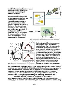
ABSTRACT We have carried out measurements of electromigration-induced strains in copper conductor lines using microbeam energy dispersive x-ray diffraction. Strains developed in random texture damascene Cu 2µm-wide, 0.16 µm-thick conductor lines with TaN liners in low-k dielectric during electromigration at 350ºC are much smaller than electromigration-induced strains in (111) fiber texture Al-on-Si, 10µm-wide, SiO2 passivated conductor lines. The reasons for these differences in electromigration behavior may involve the different roles of grain boundary and interface diffusion paths and the different passivation structures and materials for the two types of samples. INTRODUCTION Cu interconnects have achieved improved conductivity and longer electromigration lifetime in integrated circuits. However, because interconnect dimensions are becoming smaller and smaller, electromigration remains an important reliability issue. In the usual view of electromigration in a polycrystalline conductor line, when current flows through the conductor line, metal atoms move from cathode to anode due to the flux of electrons. The atoms pile up at the anode end, and a stress gradient builds up along the conductor line. Aluminum conductor lines have been studied [1], where grain boundary diffusion dominants during electromigration, and biaxial stress is formed for a wide line. However, electromigration in Cu is believed to involve mainly surface diffusion rather than grain boundary diffusion.[2] Korhonen et al.[3] developed an approximate analytical model to predict the strain developed in a passivated conductor line during electromigration. Hau-Riege et al.[4] used finite element techniques to calculate the effective bulk modulus for Cu conductor lines with liners and dielectric layers, to analysis the stress developed by electromigration. However experimental measurements of electromigration induced stress for Cu have not been reported. This paper presents measurements of electromigration induced strain for Cu conductor lines and comparisons to the strain values calculated using the approach of Korhonen et al.[3] SAMPLES AND EXPERIMENTS The experiments were conducted at the National Synchrotron Light Source (NSLS) at Brookhaven National Lab. Cu conductor line samples made by the dual damascene process were prepared at IBM. Figure 1.(a) shows a sample with three Cu lines in parallel with 0.2µm separation. Three sections of 100µm long lines are connected in series. The thickness of the Cu lines is 0.16µm. TaN is a diffusion barrier on the bottom and sides of the lines. On the top of the lines, there is a SiCxHyNz 20nm thick passivation layer. A 100µm SiO2 layer was
Data Loading...


