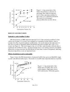
Grain-Scale Strain and Orientation Measurements during Electromigration in Al Conductor Lines by Synchrotron X-Ray Micro
- PDF / 402,609 Bytes
- 6 Pages / 612 x 792 pts (letter) Page_size
- 35 Downloads / 355 Views
1027-D01-04
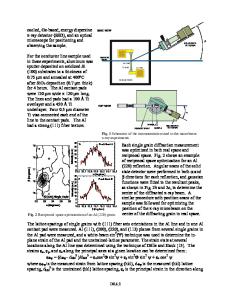
Grain-Scale Strain and Orientation Measurements during Electromigration in Al Conductor Lines by Synchrotron X-Ray Microbeam Diffraction Hongqing Zhang1, G. S. Cargill1, Youzhang Ge2, A. M. Maniatty2, and Wenjun Liu3 1 Materias Science and Engineering, Lehigh University, 5 E Packer Ave, Bethlehem, PA, 18015 2 Mechanical, Aerospace and Nuclear Engineering, Rensselaer Polytechnic Institute, Troy, NY, 12180 3 Advanced Photon Source, Argonne National Laboratory, Argonne, IL, 60439 ABSTRACT Al conductor lines, with Ti-Al top and bottom layers and SiO2 passivation, were stressed with current density 1.5 × 10⁶ A/cm2at 190ûC, and the strains developed during electromigration were measured in-situ by white and monochromatic beam synchrotron x-ray microdiffraction. Grain-scale deviatoric strain measurements with 0.4µm beam size and perpendicular full strain measurements with 1.0µm beam size were made repeatedly during electromigration. A strong strain gradient developed along the upstream half of the conductor lines during electromigration, although no resistance changes, voids or extrusions were seen. Orientation maps showed near-bamboo grain structure. Results from an approximate analytic model, using the Eshelby inclusion theory, are consistent with the measurement results for late-stage electromigration-induced strains. BACKGROUND Strains and stresses formed in conductor lines during eletromigration (EM) have caused reliability problems in microelectronic devices with the shrinking size of the devices. Synchrotron x-rays have been used to study strains in conductor lines. Wang et al. [1] used synchrotron x-rays to study the EM-induced strains in SiO2 passivated Al conductor lines with 10µm spatial resolution, and they found that a linear strain gradient formed during EM. Valek et al. [2] used a smaller, 0.8µm x-ray beam to study EM in Al conductor lines, and they found evidence of plastic deformation in the downstream end of the lines during EM. Analytical models have been developed and tested for strain evolution during EM in Al conductor lines [1, 3]. It is generally accepted that EM in polycrystalline Al lines occurs mainly along grain boundaries [4]. The passivation layer and surrounding matrix play an important role in determining the magnitude of EM induced strains, as reported finite element calculations by Hau-Riege et al. [5]. In this paper, we use synchrotron x-ray microdiffraction to investigate strain evolution in Al conductor lines during EM, and we describe a model to interpret the experimental data based on the near-bamboo microstructures of the Al conductor lines. SAMPLES AND EXPERIMENTS Al conductor lines with Ti-Al top and bottom layers and SiO2 passivation were studied. The lines were 30µm long, 2.6µm wide and 0.75µm thick, as shown in the cross section sketch in Fig. 1. The TEM image in Fig. 2, obtained from a thin cross section of a conductor
line with the same thermal history as those used for the x-ray studies, shows that the Al lines consist of large, micron-scale columnar grains, ~2
Data Loading...