Thermal Interactions of Ni on Stepped 6H-SiC Surfaces: Implications for Thin Film Microstructure
- PDF / 330,078 Bytes
- 6 Pages / 612 x 792 pts (letter) Page_size
- 11 Downloads / 250 Views
0911-B10-03
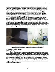
Thermal Interactions of Ni on Stepped 6H-SiC Surfaces: Implications for Thin Film Microstructure Andrew A Woodworth1, Srikanth Raghavan2, and Charter D Stinespring1 1 Department of Chemical Engineering, West Virginia University, 403 Engineering Sciences Building, Morgantown, WV, 26501-6102 2 Lane Department of Computer Science and Electrical Engineering, West Virginia University, Engineering Sciences Building, Morgantown, WV, 26506-6109 ABSTRACT Ni films are widely used in high temperature SiC-based electronic devices. The experiments reported here compare the thermal behavior of Ni films deposited on standard 6HSiC (0001) surfaces with films deposited on periodically stepped surfaces. The former were prepared by wet chemical etching and are typical of those used in device fabrication. The latter were prepared by high temperature hydrogen etching. Ni films ranging from monolayer to nominal device thickness (~50 nm) were annealed at 700 oC on both surfaces. Analysis of these surfaces by in-situ Auger electron spectroscopy (AES) and ex-situ atomic force microscopy (AFM) provided elemental, chemical and morphological information. The results show that the morphology and surface composition of annealed films are dependent on initial film thickness and substrate surface conditions.
INTRODUCTION SiC is a robust, wide band gap semiconductor suitable for fabricating high power / temperature devices [1]. Because of nickel’s high melting point (1455 oC) and ability form Schottky barriers [2,3] and Ohmic contacts [4] its use in SiC-based electronics has been studied extensively [5]. Based on bulk work function and electron affinity data, Ni is predicted to form a Schottky barrier on SiC.[6-8] Experimentally, Ni/SiC Schottky junctions are observed to become Ohmic after being annealed at 900 oC. This has been attributed to thermally induced changes in the junction microstructure which begin to occur with the formation of Ni-silicide at 600 oC [9]. The Schottky junctions have a Ni-silicide/C/SiC structure, while the Ohmic junctions have a C/Ni-silicide/C/SiC structure [10]. Clearly, interdiffusion and reaction are important even at relatively low temperatures. In our application, we are concerned with the development of high temperature gas sensors that operate in the range of 500 oC – 700 oC. Therefore, it is important to understand those factors that influence the microstructure of the metal-semiconductor interface, particularly at the higher temperature limit. Currently SiC devices are fabricated on surfaces that are highly polished by the vendor and then degreased and wet chemically cleaned. The purpose of the last two steps is to remove surface oxides and other contaminants. These “standard surfaces” have a high density of defects related to the polishing process that may enhance diffusion and intermixing at the Ni/SiC interface. High temperature hydrogen etching can be used to remove this damaged material and yields periodically “stepped surfaces” with unit cell high steps and atomically flat terraces several
Data Loading...