Thermodynamics and Growth of GaN Single Crystals Under Pressure
- PDF / 2,338,309 Bytes
- 12 Pages / 414.72 x 648 pts Page_size
- 30 Downloads / 359 Views
of interest as optimum materials for short wave length optoelectronics and high temperature electronic applications. Currently, thin layers of these compounds are grown on foreign substrates [1,2] by Molecular Beam Epitaxy and Metalo Organic Chemical Vapor Deposition. Both n- and p-type layers can be crystallized and the commercial blue diode based on InGaN/GaN is now available. Very recently [3], Nakamura and his group have demonstrated that GaN based, room temperature operating laser diode can be constructed on heteroepitaxially grown GaN layer structure. This proves that GaN is an excellent material for short wave length optoelectronics. However it was shown that the layers on sapphire or SiC substrates grow as columns of perfect crystallites separated by dislocations forming low angle boundaries. The lowest Table I Melting conditions for III-N compounds nitride AIN GaN InN
TM*, K theory PN2 kbar -3500 [5] 0.2[7] -2800[5] 45[8,9] -2200[5,6] 60[6]
dislocation density for heteroepitaxial layers of GaN is as high as 108 /cm 2 [4]. The homoepitaxial growth of layers on nitride single crystalline substrate is the best way to reduce the dislocation density. Unfortunately, bulk crystals of nitrides cannot be obtained by known methods such as Czochralski or Bridgman growth from stoichiometric melts.
349 Mat. Res. Soc. Symp. Proc. Vol. 499 ©1998 Materials Research Society
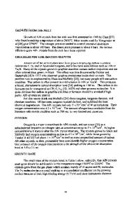
This is due to extremely high melting temperatures and very high decomposition pressures at melting (Table 1). Growth of semiconductor quality crystals at these conditions would be practically impossible. Therefore the crystals have to be grown by methods requiring lower temperatures. In our experiments we use the high temperature solution method to grow A'IIN crystals from liquid Al, Ga and In. THERMAL STABILITY OF AIN, GaN, InN Comparing temperature dependences of the Gibbs free energy G(T) of nitrides and their constituents we can illustrate the analogies and differences in the properties of AIN, GaN and InN. In Fig. 1, we have shown G(T) curves [10,11] for III-V nitrides and their constituents, for N 2 pressure of 1 bar. The reference state for G(T) is the sum of energy of one mole of gas
of metal atoms and 1 g.at. of atomic nitrogen, i.e. the reference state for bonding energies. temperature, K temperature, K 1000 2000 3000 0 1000 2000 3000 0 100
A
300
200
0
1-100
E -100
Al
................. 1/2N 2
a)-200
21 -200 (D
a)
(D
.0-300 (D
GaN
a)
AI+1/2N2
A[N
Ga .. ............ N .... .. . .... 1/2 N2
F
-300
G(
Eb(GaN)
Eb(AIN)
Ga + 1/2N 2 -400
a b temperature, K 0
0or
1000
2000
temperature,K
3000
0 R
a)
0
E
0
2000
--
100-
50 .
(D -200
tj-200
Me+1/2N 2 GaN
1ba
""N-. .-0
3000
-50.
0
"-100
1000
1kbar
S-300 -350-
CD
d c Fig. 1 Gibbs free energy change with temperature for III-V nitrides and their constituents: (a), (b) and (c) - for N 2 pressure of 1 bar, (d) - G(T) for the constituents is the sum of averaged energy of the metal and the free energy of nitrogen at pressure of I bar and 11 kbar. 350
AI
Data Loading...