Thermoelectric Nanowires By Template Synthesis: Fabrication, Contacts and Properties
- PDF / 1,039,042 Bytes
- 6 Pages / 612 x 792 pts (letter) Page_size
- 93 Downloads / 351 Views
H7.24.1
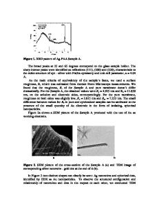
Thermoelectric Nanowires By Template Synthesis: Fabrication, Contacts and Properties Oded Rabin (a), Yu-Ming Lin (b), Stephen B. Cronin (c), Gang Chen (d), Mildred S. Dresselhaus (b,c) Massachusetts Institute of Technology, Cambridge, MA 02139, U.S.A. (a) Dept. of Chemistry. (b) Dept. of Electrical Engineering and Computer Science. (c) Dept. of Physics. (d) Dept. of Mechanical Engineering. ABSTRACT Using the technique we have developed to grow porous anodic alumina (PAA) templates on the surface of silicon wafers, we have fabricated arrays of nanowires of thermoelectric materials. By this method we can control both (1) the in-plane geometry by the design of the template and the substrate, and (2) the out-of-plane dimension by control over the electrochemical nanowire growth process. We use several straightforward methods to make electrical contacts to the nanowires. Our transport studies show that both the structure of the nanowire and the contact region have a strong influence on the observed properties of the arrays. INTRODUCTION Nanoscience has seen significant progress in the last decade, in developing techniques that are increasingly precise in their ability to build nanostructures, such as quantum wells, quantum wires and quantum dots. Simultaneously, analytical tools were adapted to investigate this fascinating regime and characterize the unusual properties of these structures. Theory has also played an important role in guiding the experimental efforts, and in the prediction and understanding of the new phenomena that come to light in the quantum limit. One example of the impact that such new advances have made is the recent developments in the field of thermoelectrics. Traditionally, material science was the tool used to discover new and improved thermoelectric materials. Today it is accepted that size effects are important, and low-dimensional systems are being explored for their potential to exceed the thermoelectric (TE) performance of their constituent materials in bulk form. According to theoretical studies, the enhancement of the thermoelectric figure of merit, Z, in nanostructures is related to the increase in the electronic density-of-states, the removal of the minority carriers, and the selective scattering of phonons over charge carriers. [1,2] Recently, an increase in Z values was reported for superlattices [3], and quantum-dot superlattices [4], and increased Seebeck coefficient values were measured in nanowire arrays. [5] σ ⋅S2 Z= (Equation 1) κ Thermoelectric devices make use of the coupling of the electrical current to the thermal current in the body of the material for power generation or for cooling purposes. [6] Such a device is composed of junctions of thermoelectric materials, which are characterized by the thermoelectric figure of merit, Z, a function of the electrical conductivity (σ), the Seebeck coefficient (S), and the thermal conductivity (κ) of the materials (Equation 1). The development of materials of high Z is a focus of on-going research. Theoretical studies predict t
Data Loading...


