Thermomechanical Behavior and Properties of Passivated Pvd and Ecd Cu Thin Films
- PDF / 337,570 Bytes
- 6 Pages / 595 x 842 pts (A4) Page_size
- 92 Downloads / 309 Views
O4.5.1
THERMOMECHANICAL BEHAVIOR AND PROPERTIES OF PASSIVATED PVD AND ECD Cu THIN FILMS M. Gregoire 1, S. Kordic 2, P. Gergaud 3, O. Thomas 3, and M. Ignat 4 1
STMicroelectronics, Crolles2 Alliance, 850 rue Jean Monnet, 38926 Crolles, France Philips Semiconductors, Crolles2 Alliance, 860 rue Jean Monnet, 38920 Crolles, France 3 TECSEN, CNRS, Université of Aix-Marseille III, Faculté St Jérôme, 13397 Marseille, France 4 LTPCM-INPG, CNRS, Domaine Universitaire, BP 75, 38402 St Martin d’Hères, France 2
ABSTRACT The thermomechanical behavior is investigated of SiCN-encapsulated blanket Physical Vapor Deposited (PVD) and Electrochemically Deposited (ECD) Cu films. At lower ECD Cu film thicknesses an anomalous shape and a tail of the stress-temperature curve are observed, which are not caused by impurities at the interfaces, but are correlated to highly textured microstructure. Repeated thermal cycling of up to 400 oC does not markedly change the texture of the films, but a significant texture change takes place with increasing ECD Cu thickness. Thermal cycling induces grain growth for thicker films only. Impurity content and distribution in the PVD films do not change due to cycling. INTRODUCTION Copper thin films fabricated using Physical Vapor Deposition (PVD) and Electrochemical Deposition (ECD) are widely used in modern integrated circuits (IC’s), yet the majority of studies up until now deal with sputtered Cu films. In contrast to sputtered films, Cu films fabricated with ECD techniques have a high content of contaminants, which influence film properties. It is well known that high internal stresses in films used in IC’s can lead to important failure mechanisms such as dielectric cracking, interfacial delamination, and stress voiding [1, 2]. In addition, IC’s (Figure 1) are subjected to thermal cycles during manufacturing, and during the Cu6 Dielectric
Cu5 Cu4 Cu3 Cu2 Cu1
Stress (MPa)
Cu
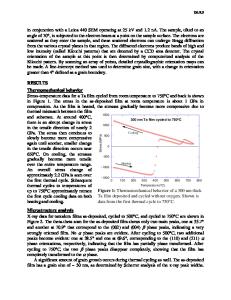
Passivated 150 nm Cu PVD film 800 600 400 200 0 -200 -400
First cycle Second cycle Third cycle
0
Figure 1. A scanning electron microscope cross section of a 65 nm design rule, 6 ECD Cu metal level interconnect, with a low relative permittivity dielectric (εr =3).
100 200 300 400 Temperature (°C)
500
Figure 2. Stress as a function of temperature determined using substrate curvature technique for the encapsulated PVD Cu stack. Sample was subjected to three thermal cycles.
O4.5.2
normal IC use. Prediction and improvement of thin film reliability require detailed knowledge of their thermomechanical behavior. To determine the stress in films during thermal cycling, the substrate curvature technique is used [3]. The impact of passivation [1, 4-5], texture [6-8], and thickness [8-9] on the stresstemperature behavior have been studied on sputtered Cu films, and marked changes in the stresstemperature curve have been observed if Cu was intentionally contaminated with oxygen [5, 10]. In this paper, the thermomechanical behavior of encapsulated PVD and ECD Cu thin films is investigated, which were deposited on a PVD Ta/TaN diffu
Data Loading...