Thickness Dependent Tetragonal Relaxation of Iron in Epitaxial Fe/Pd Multilayer Films
- PDF / 1,770,213 Bytes
- 6 Pages / 411.12 x 635.4 pts Page_size
- 12 Downloads / 248 Views
Mat. Res. Soc. Symp. Proc. Vol. 619 © 2000 Materials Research Society
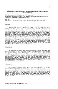
(a)
[)
Alternating Fe and Pd layers
.... [110]
(001) Fe0] (001) (1120,/• "•'"
[0001]
AI03 2
.nm
4-- Pd .4-.Sapphire
Figure 1: (a) Schematic representationof the epitaxial relationshipbetween the sapphire substrate, the Pd layers, and the Fe layers. (b) TEM image of a cross section of a (Fe2.sn/Pd4nm)32 multilayerfilm. The arrow indicatesa step with a height of afew nm in the buffer layer. The ultra-thinFe seed layer between substrate and Pd buffer is not indicated. Deposition rate and layer thickness are monitored by quartz crystal oscillators, which are calibrated utilizing an optical interference method. Epi-ready polished a-A120 3 (sapphire) single crystals, which are cut parallel to the c-axis (a-plane, (11-20)), are used as substrates. The (Fe/Pd) ML stacks are grown onto Pd buffer layers, which are pre-seeded with Fe. In order to obtain growth along the [001] direction within the buffer and the ML stack, a thin Fe layer with a thickness tFe,sed =-0.5 nm is deposited onto the sapphire substrate at temperatures 300 K _•Tseed 700 K. A Pd film with a thickness tpd = 30 nm is then evaporated at temperatures Tbuf =_700 K, and we have shown that these buffer layers grow epitaxially with a strong (001) orientation [5]. To avoid interdiffusion between adjacent layers, the alternating Fe and Pd layers are deposited at room temperature (RT). The ML stack is always terminated by a Pd layer to prevent it from oxidation when being exposed to ambient conditions e.g. for ex-situ investigations. The growth of the films is monitored by means of in-situ RHEED measurements. Ex-situ characterization is done by means of X-ray diffraction (XRD) experiments utilizing Co-ke radiation (k = 0.17902 nm). The films are also investigated by means of (high resolution) transmission electron microscopy ((HR)TEM) on cross sections of the MLs. We use a Philips CM 12 (LaB 6 cathode, 120 kV) for conventional TEM. A JEOL 2010F microscope (field emission gun, 200 kV, Degussa AG, Hanau) has been used for HRTEM investigations. Magnetization measurements at low temperatures in external field of up to 50 kOe are carried out utilizing a SQUID magnetometer (Superconducting QUantum Interference Device. Type Quantum Design MPMS-XL5). RESULTS AND DISCUSSION In the present work we investigate a series of (Fet/Pd4nm)32 ML films consisting of 32 bilayers of Fe and Pd, which are grown epitaxially onto a Pd-buffered sapphire substrate according to the recipe described above. Within this series the nominal Pd layer thickness is kept constant at tpd = 4 nm, while the Fe layer thickness is varied in the range 0.5 nm < t < 3 nm. Figure 1 shows (a) a schematic drawing of the epitaxial relationship between the sapphire substrate and the Pd and Fe layers as evidenced from RHEED measurements [4,5] and (b) a conventional TEM image of a cross-sectionally prepared (Fe2.snm/Pd4nm)32 ML. The layered structure of the ML film is clearly visible from the alternating (atomic number) Z-contrast in t
Data Loading...