Thin-Film Transistors in CO 2 -Laser Crystallized Silicon Films on Fused Silica
- PDF / 1,554,262 Bytes
- 7 Pages / 417.6 x 639 pts Page_size
- 63 Downloads / 308 Views
THIN-FILM TRANSISTORS IN C0 2-LASER CRYSTALLIZED SILICON FILMS ON FUSED SILICA N. M. Johnson, H. C. Tuan, M. D. Moyer, M. J. Thompson, D. K. Biegelsen, L. E. Fennell, and A. Chiang Xerox Palo Alto Research Centers, Palo Alto, CA 94304 ABSTRACT Thin-film transistors (TFT) have been fabricated in scanned CO 2 laser-crystallized silicon films on bulk fused silica. In n-channel enhancement-mode transistors, it is demonstrated that an excessively large leakage current can be electric-field modulated with a gate electrode located beneath the silicon layer. This dual-gate configuration provides direct verification on bulk glass substrates of back-channel leakage as has recently been demonstrated for beam-crystallized silicon films on thermal oxides over silicon wafers. With the application of deep-channel ion implantation to suppress back-channel leakage, high-peformance TFTs have been fabricated in single-crystal silicon films on fused silica. The results demonstrate that scanned CO 2 laser processing of silicon films on bulk glass can provide the basis for a silicon-on-insulator technology. INTRODUCTION Beam-crystallized silicon layers on bulk glass substrates have been used to fabricate thin-film transistors (TFTs) [1,2]. While the semiconducting layer has generally possessed large-angle incoherent grain boundaries which limit device performance [3,4], high-performance transistors have recently been reported for films containing predominantly subgrain boundaries and crystallized with a swept graphite strip-heater [5] and for single-crystal silicon films crystallized with a scanned CO 2 laser [6]. An additional mechanism which has been found to limit performance in n-channel metal-oxide-semiconductor (MOS) TFTs is back-channel current leakage, due apparently to a high density of residual positive space charge in the dielectric substrate [7]. This mechanism has been successfully suppressed by using deep-channel ion implantation to prevent the formation of a conducting inversion layer along the back interface of the silicon layer [5,7]. In this paper are presented results from a study of transistors fabricated in CO 2 laser-crystallized silicon films on bulk fused silica. In n-channel enhancement mode devices, it is shown with dual - gate test devices that an excessively large leakage current can be electric-field modulated with a gate electrode located beneath the silicon layer. This provides direct verification on bulk glass substrates of back-channel leakage. High - performance TFTs were fabricated on bulk fused silica by using deep-channel ion implantation to suppress back-channel leakage and laser-crystallized Mat.
Res.
Soc.
Symp.
Proc. Vol.
13 (1983)(
Elsevier Science Publishing Co.,
Inc.
606
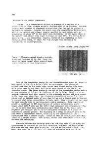
single-crystal silicon films to eliminate the detrimental effects of residual grain boundaries on device operation. DEVICE FABRICATION Conventional microelectronic processing techniques were combined with laser crystallization to fabricate thin-film silicon transistors. In this section is summarized the processing ste
Data Loading...