NMOS Logic Circuits in Laser-Crystallized Silicon on Quartz
- PDF / 1,762,008 Bytes
- 8 Pages / 417.6 x 639 pts Page_size
- 50 Downloads / 307 Views
NMOS LOGIC CIRCUITS IN LASER-CRYSTALLIZED
SILICON ON QUARTZ
A. CHIANG, M. H. ZARZYCKI, W. P. MEULI, AND N. M. JOHNSON
Xerox Palo Alto Research Center, 3333 Coyote Hill Road, Palo Alto, CA 94304 ABSTRACT
Depletion mode as well as enhancement mode n-channel thin-film transistors (TFT's) have been fabricated in CO 2 lasercrystallized silicon on fused quartz. Nearly defect-free islands were obtained by using an offset circular beam to form a tilted melt interface. The optimization of subsequent processing steps to achieve simultaneously low leakage currents and voltage thresholds appropriate for depletion-load NMOS circuits involved adjustments of ion implantation and high temperature cycles with the aid of simulation. The resultant high performance silicon-gate TFT's have led to NMOS ring oscillators with 2.5 ns delay/stage and dynamic shift registers with MHz clock rates. These are the first logic circuits fabricated in beam-crystallized silicon on bulk amorphous substrates. INTRODUCTION
Silicon thin film devices on bulk glass have been of great interest to such largearea electronic technologies as flat panel displays and image sensors which require transparent substrates with unlimited size [1,2,3,4]. With the demonstration of high performance devices built in laser-crystallized defect-free silicon material on fused quartz [5,6], application of such TFT's can now reach beyond local switching of
individual transducers into the realm of logic circuits having sufficiently high speed for the data rates often encountered in image processing [7]. It is known that n-channel TFT's exhibit tensile stress-enhanced electron mobility due to differential thermal contraction between silicon and quartz [5]. We have thus chosen to develop an NMOS process for silicon-on-glass because of the stressenhanced electron mobility and the small number of masking steps to facilitate application of laser-crystallized silicon on quartz to large-area-electronics. In this paper, we report on our work which has led to the first realization of logic circuits in silicon on bulk glass. A technique for laser-crystallization with a tilted meltzone to obtain nearly defect-free Si material for fabrication of high performance devices is described first. The subsequent optimization of an NMOS process is then discussed with emphasis on fine tuning a double boron ion implantation process and the following high temperature cycles to achieve simultaneously voltage thresholds and low leakage currents appropriate for 5-V NMOS logic circuits. LASER CRYSTALLIZATION
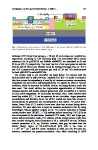
Crystallization of silicon thin films on quartz in the encapsulated and patternedstriped configuration by a scanned CW CO 2 laser has been reported previously [8]. With a solidification front tilted relative to the direction of molten zone path, structural defects can be greatly reduced or even eliminated by a lateral defect-sinking effect. Mat. Res. Soc. Symp. Proc. Vol. 23 (1984) @Elsevier Science Publishing Co., Inc.
552
Very high percentage of (100) oriented device islands with no sub-gra
Data Loading...