Time-Dependent Forming Characteristics in Pt/NiO/Pt Stack Structures for Resistive Random Access Memory
- PDF / 292,981 Bytes
- 6 Pages / 432 x 648 pts Page_size
- 107 Downloads / 459 Views
Time-Dependent Forming Characteristics in Pt/NiO/Pt Stack Structures for Resistive Random Access Memory Yusuke Nishi, Tatsuya Iwata, Daisuke Horie and Tsunenobu Kimoto Department of Electronic Science and Engineering, Kyoto University, Kyotodaigaku-katsura, Nishikyo, Kyoto, 615-8510, Japan ABSTRACT Constant voltage Time-Dependent Forming (TDF) measurements in as-deposited Pt/NiO/Pt stack structures have been conducted. From TDF characteristics, formation of conductive filaments at forming process by applying voltage follows weakest link theory. Furthermore, weakest spots are almost randomly distributed in NiO thin films according to Poisson statistics, each of which can contribute conductive paths locally generated. A “percolating layer” in which the conductive filaments percolate by applying voltage may exist in the NiO thin film. The thickness of the layer is much smaller than that of NiO thin films. INTRODUCTION In recent years, Resistance Switching (RS) phenomena in metal/oxide/metal stack structures attract much attention to application of Resistive Random Access Memory (ReRAM) as the next-generation nonvolatile RAMs, which may replace flash memories. ReRAMs using binary Transition Metal Oxides (TMOs) such as NiO [1,2], TiO2 [3,4], or CoO [5] possess many advantages of low-power, high-speed operation, high on/off ratio and compatibility with complementary metal-oxide-semiconductor (CMOS) technologies. Despite announces about starting production of ReRAM by some companies, issues for practical use of ReRAM remains unchanged. Clarifying universal mechanism of RS and developing distribution control process of characteristic values of RS have been required. In metal/TMO/metal stack structures, the formation and rupture of conductive filaments have been widely accepted as a RS mechanism. Forming process in these structures by conductive filament exhibits some analogy to Soft BreakDown (SBD) of SiO2 in MOS structures. Time-dependent dielectric breakdown (TDDB) is a useful method for the analysis of failure mechanism in MOS structure, which is based on percolation paths formed by defects due to electrical stress [6]. In the present study, we assume a conductive filament model in forming process. Constant voltage Time-Dependent Forming (TDF) characteristics instead of TDDB in as-deposited Pt/NiO/Pt stack structures are investigated. Similarity and Dissimilarity of conductive filaments in NiO thin films to percolation paths in SiO2 thin films are discussed by comparing TDF characteristics to TDDB.
141
EXPERIMENT NiO thin films were deposited on Pt(100 nm)/Ti(5 nm)/SiO2(200 nm)/p-Si substrates by a reactive radio-frequency (RF) sputtering method using a Ni target of 99.99% (4N) purity [7]. The total pressure, substrate temperature and RF power during sputtering were kept at 0.6 Pa, RT and 100 W, respectively. The proportion of O2 flow rate in the Ar + O2 gas mixture was 5%. The thickness of NiO thin films (dNiO) was varied from 30 nm to 100 nm. Pt Top Electrodes (TEs) with diameters (I) in the range from 50 Pm to 500
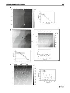
Data Loading...