Transmission Electron Microscopy Study of an Epitaxial Gate Oxide on III-N Semiconductor Structures
- PDF / 739,807 Bytes
- 6 Pages / 612 x 792 pts (letter) Page_size
- 57 Downloads / 320 Views
E11.21.1
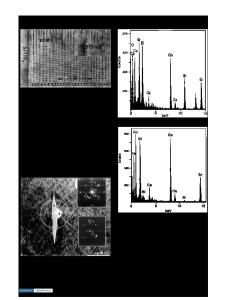
Transmission Electron Microscopy Study of an Epitaxial Gate Oxide on III-N Semiconductor Structures Yoga.N. Saripalli, X-Q Liu, D.W. Barlage(1), M.A.L. Johnson, D. Braddock(2), N.A. Stoddard, A. Chugh Department of Material Science and Engineering, NC State University, Raleigh, NC 27695. (1) Department of Electrical and Computer Engineering, North Carolina State University (2) OSEMI, Inc Rochester, MN ABSTRACT An effective gate insulator for compound semiconductors has been a challenging goal for the materials research community for nearly 40 years. Recent developments on the epitaxial deposition of complex gate oxides as gate insulators have shown promise with the demonstration of enhancement mode high electron mobility transistors (e-mode HEMTs). In this work, gate oxide epilayers deposited on III-V semiconductors for field effect transistors (III-V MOSFETs) are examined using transmission electron microscopy (TEM) to identify the structure of the oxide/semiconductor interface. The high resolution images of the cross-sectional structures for the first time reveal a crystalline nature of the interface between the oxide and the III-V semiconductor. The composition of the oxide layers are determined by Z-contrast Electron Energy Loss Spectroscopy (EELS). The surface morphology of the FET structures is investigated by atomic force microscopy (AFM) both before and after gate oxide deposition, and the structural results are related to device DC electrical characteristics. With an underlying GaN/InGaN heterojunction grown by metal-organic chemical vapor deposition (MOCVD) on sapphire, the MOSFET devices exhibit the characteristics of a substantially unpinned interface, including the capacity for significant charge accumulation and transconductance at positive gate voltages. INTRODUCTION The scaling of transistors to nanoscale gatelengths is driving an increasing demand for developing high-k dielectrics thin films over semiconductors [1]. The requirements for the dielectric layer that is grown include high dielectric constant, band gap, conduction band offset, low oxygen diffusivity, thermodynamic stability and most importantly a very high quality interface with minimum interfacial states density (Dit) and low gate leakage current Thermal stability is another important problem as the devices are scaled to low size-scales. As a potential alternative to Silicon, III-V compound semiconductors offer high thermal stability, high speed and high power switching [1-6]. In the case of fabricating transistors based on III-V compound semiconductors, growth of a high quality insulating layer under the gate has always been a limitation. Many insulating layers like Ga2O3, Ga2O3 (Gd2O3), Y2O3, Sc2O3, MgO, thermally oxidized GaN film, have been tried both on GaAs and GaN based transistors [2-14]. Recently, epitaxially deposited Ga2O3 and Ga2O3(Gd2O3) have been studied for the fabrication of III-V compound transistors. Both the oxides provide very good quality dielectric with
E11.21.2
reduced defect densities and interfacial
Data Loading...


