Transmission Electron Microscopy Study of Thick Copper-304 Stainless Steel Multilayers
- PDF / 2,930,524 Bytes
- 6 Pages / 414.72 x 648 pts Page_size
- 35 Downloads / 276 Views
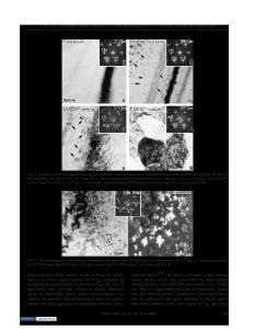
TRANSMISSION ELECTRON MICROSCOPY STUDY OF THICK COPPER-304 STAINLESS STEEL MULTILAYERS M. A. WALL, T. W. BARBEE, Jr. AND T. WEIHS Lawrence Livermore National Laboratory Chemistry and Materials Science Department Livermore, CA U.S.A. 94550. ABSTRACT Thick (10 to 25 gim), free-standing, equal layer thickness, Copper(Cu)-304 Stainless Steel(SS) multilayer foils, having periods of lnm to 100 nm, synthesized by magnetron sputter deposition, have been examined by plan view and cross-sectional transmission electron microscopy. Multilayer growth morphology, individual layer structure and crystallographic phase orientation relationships were characterized in this study. Electron Energy Loss filtered imaging of a 20 nm period multilayer cross-section was also performed and showed that nickel had diffused into the Cu layers from the SS during synthesis. X-ray powder diffraction scans were performed and analyzed. A pure deposit of 304SS was synthesized and had a metastable BCC structure. Multilayer samples having periods of 20 nm were found to have a coherent layered Cu(FCC)SS(FCC) structure. At larger periods (50 & 100 nm) a bimodal Cu(FCC)-SS(FCC & BCC) structure was formed. These observations show that the 304SS will grow with a metastable BCC structure when sputter deposited. When layered with Cu(FCC) the 304SS has its equilibrium FCC structure at layer thicknesses up to 10nm as a result of epitaxy with the copper. At larger SS layer thicknesses the SS appears to locally transform to the metastable BCC structure during synthesis, refining the grain structure of the depositing SS layer and the subsequent Cu layer. This transformation significantly increases the strength of the larger period multilayer. INTRODUCTION Multilayers are dense ultra-fine grained high interface concentration solids. As a result of the atomic level structural and chemical control provided by multilayer synthesis techniques, materials having unique structures and physical properties not accessible by conventional processing may be created. Transmission Electron Microscopy (TEM) characterization provides important information enabling correlation of the atomic level structure and the properties of these nano-structured materials. These correlations are clearly important in the development of new multilayer materials of technological importance. Current multilayer applications include x-ray and neutron optics, protective coatings, magnetic thin films, integrated circuit interconnects and potentially, structural components. Reported TEM characterization of multilayered films has been primarily for samples < 1 gim thick [1,2]. Recent advances in multilayer synthesis technology have made possible fabrication of substantially thicker multilayer structure foils (>250 jim thick). In the past, multilayer characterization has emphasized interfaces in multilayer materials (i.e. interface morphology, structure, chemical abruptness and stability). The increase in multilayer thickness from film dimensions (t10 gim) results in the need for characterization of multi
Data Loading...


