Two-dimensional Epitaxial Growth of Strained InGaAs on GaAs (001)
- PDF / 386,448 Bytes
- 6 Pages / 612 x 792 pts (letter) Page_size
- 85 Downloads / 332 Views
F3.19.1
Two-dimensional Epitaxial Growth of Strained InGaAs on GaAs (001) Hong Wen, Zhiming Wang, G.J. Salamo, MRSEC and Microelectronics-Photonics Program, University of Arkansas, Fayetteville, Ar 72701, U.S.A.
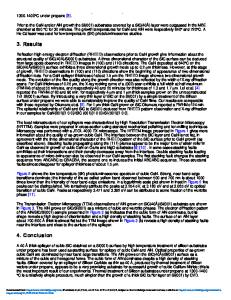
ABSTRACT Molecular beam epitaxy growth of lattice mismatched In0.53Ga0.47As / GaAs(100) system is studied by in situ scanning tunneling microscope (STM) and reflection high energy electron diffraction. InGaAs layers with a thickness ranging up to 250 nm do not exhibit a smooth surface when grown under In-rich conditions. RHEED and STM confirm the wellordered (4x2) reconstruction and mono-layer steps associated with this unique planar growth mode. Large STM scans reveal a characteristic morphology of rectangular shaped islands distributed on large flat terraces which are typically more than 300 nm width but only monolayer steps.
INTRODUCTION Indium-Arsenic (InAs) and Indium-Gallium-Arsenic (InGaAs) are widely used in electronic and photo-electronic devices such as high electron mobility transistors, laser devices, and infrared photo detectors[1-4]. The strain-driven growth of InAs on GaAs(001) under As-rich conditions can produce a morphological transformation from two-dimensional (2D) to three-dimensional (3D) and the accumulated strain is partly relieved via elastic expansion at the free surface of these 3D inlands [5-7]. Though this growth mode can be used to produce self-assembled quantum structures, dislocations formed at island edges during the later stages of growth are very likely to thread during the coalescence of neighboring islands[8,9]. It was found that by changing the growth condition from As-rich to In-rich, the initial 3D island growth can be suppressed and, hence, the dislocations are confined to InAs/GaAs interface. The suppression of 3D island growth results in the planar growth of InAs on GaAs[10]. Similar phenomenon was also observed on InP and GaP substrates[1113]. The application of this planar growth technique has contributed to striking improvements of the electronic and optical properties of these materials. In the work reported here, this growth technique is extended from InAs on GaAs to InGaAs on GaAs. The evolution of the surface morphology of In0.53Ga0.47As deposited on GaAs at different V/III flux ratios were investigated using a high-performance in situ molecular beam epitaxyscanning tunneling microscope (MBE-STM) system combined with reflection high energy electron diffraction (RHEED). The fully relaxed InGaAs /GaAs(001) 2D growth makes InP/InGaAs/GaAs one-step epitaxial growth to be possible because of the lattice match between InP and In0.53Ga0.47As.
F3.19.2
EXPERIMENT DETAILS The research was performed in a combined molecular beam epitaxy (MBE) and scanning tunneling microscopy (STM) ultra-high vacuum system. A 0.5 µm thick GaAs buffer layer was deposited at 580oC on (001)-oriented GaAs substrate. In0.53Ga0.47As epilayers were grown with a rate of 0.25 ML/s at 500oC on GaAs(001) substrates. In situ reflection highenergy electron diffraction (RHEED) studies indicated
Data Loading...