Strained InGaAs/GaAs Multiple Quantum Wells Grown on Planar and Pre-Patterned GaAs(100) Substrates VIA Molecular Beam Ep
- PDF / 1,461,772 Bytes
- 6 Pages / 420.48 x 639 pts Page_size
- 65 Downloads / 357 Views
STRAINED InGaAs/GaAs MULTIPLE QUANTUM WELLS GROWN ON PLANAR AND PRE-PATTERNED GaAs(100) SUBSTRATES VIA MOLECULAR BEAM EPITAXY: APPLICATIONS TO LIGHT MODULATORS AND DETECTORS
Li Chen, Kezhong Hu, K. C. Rajkumar, S. Guhae, R. Kapre and A. Madhukar Photonic Materialsand Devices Laboratoiy, University of Southern California, Los Angeles, CA 90089-0241
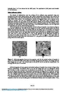
ABSTRACT We report the realization of high quality strained InGaAs/GaAs multiple quantum wells (MQW) grown on planar GaAs (100) substrates through optimization of molecular beam epitaxical (MBE) growth conditions and structure. Such MQWs containing - I1% In have lead to the realization of an asymmetric Fabry-Perot (ASFP) reflection modulator with a room temperature contrast ratio of 66:1 and an on-state reflectivity of 30%. For In composition a 0.2, the improved optical quality for very thick (>21im) InGaAs/GaAs MQWs grown on pre-patterned substrates is demonstrated via transmission electron microscopy (TEM) and micro-absorption measurements.
Strained InGaAs/AIGaAs layered structures grown on GaAs(100) substrates have attracted considerable attention for their application in vertical cavity surface emitting lasers [I], resonant tunneling diodes (RTD) [2], and light modulators [3,4]. In the transmission geometry, such modulators can take advantage of the transparent nature of the GaAs substrate so that, unlike the GaAs/AIGaAs based modulators, there is no need for a patterned removal of the GaAs substrate. Reflection mode ASFP modulators, when combined with RTDs and Si field effect transistors, provide optical digital switches with high fan-out useful for digital optical computing and communication networks [5]. In the reflection geometry, inverted reflection modulators [6] can also be made in which light passes in and out through the substrate so that a Si-chip containing control electronics can be flip-chip bonded to the modulator bearing GaAs chip [7]. When combined with arrays of strained InGaAsIGaAs lasers, detectors and Si-control electronics, analog optical neuron units can be realized. Unlike strained InGaAs/AIGaAs quantum well lasers and RTDs, which require relatively thin active layers, the major requirement for light modulators is to grow the strained active region to thicknesses (-1.5Ipm) necessary to obtain reasonable optical interaction path length. Through control of the growth kinetics via reflection high-energy electron diffraction (RHEED) pattern and intensity dynamics [81 in molecular beam epitaxical (MBE) growth, we have realized sharp exciton linewidths in such multiple quantum wells and thus achieved a typical absorption modulation per well, (Aa dw,) of - 0.004 in the exciton tail region at relatively low bias (- 80 kV/cm) [4]. Placing these strained MQWs in an ASFP configuration involving integrated Bragg mirrors it should thus be possible to obtain high contrast ratios. Contrast ratios of > 100:1 have been demonstrated [9,10] in the AIGaAs/GaAs system but have been limited to
* Present address: IBM T. J. Watson Research Center, Yorktown Height,
Data Loading...