Up Close: Center for Advanced Materials Processing at Clarkson University
- PDF / 1,639,301 Bytes
- 3 Pages / 604.8 x 806.4 pts Page_size
- 15 Downloads / 323 Views
The Center for Advanced Materials Processing (CAMP) was established in 1985 by Clarkson University in Potsdam, New York. At that time, nearly half of the research at Clarkson was materials-related but was conducted in seven separate departments of science and engineering. To coordinate and encourage this strong materials program, CAMP was created as an interdisciplinary center dedicated to research on high-technology materials processing. The current corporate sponsors of CAMP are Corning Incorporated, Eastman Kodak, Xerox Corporation, and IBM. Thèse and over 30 other industrial members support individual research projects. In 1987 the New York State Science and Technology Foundation designated CAMP as the New York State Center for Advanced Materials Processing, entitling CAMP to $1 million per year in operating funds. In addition, CAMP is supported by fédéral and University sources. In its rôle as an éducation and research initiative, CAMP has three goals: 1. Enhance Clarkson University's expertise and réputation as a center of excellence in materials processing research. 2. Greatly increase the mutually bénéficiai relationships between industrial organizations and the University; and 3. Strengthen graduate and undergraduate éducation in materials processing. Research at CAMP Innovative research by Egon Matijevic, Distinguished University Professor, has contributed greatly to the development of the fundamental principles for the formation and interactions of colloidal disper-
MRS BULLETIN/FEBRUARY1990
sions. Using Matijevic's work as a foundation, CAMP has developed four programs in high-technology materials research: electronic materials processing, fine-particle processing, particulate control in process equipment, and polymer processing.
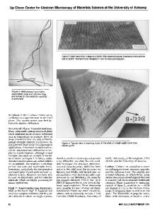
Electronic Materials Processing (S.V. Babu, Director of Research) The electronic materials processing group is exploring thin film déposition and etching, bulk crystal growth, and device characterization. Researchers are investigating new materials and processes that will enhance the performance of very large scale intégration devices and packages; new device structures also are being developed. Each of the research projects listed below deals with the characterization or processing of materials that are intégral to an electronic device or package. • Déposition of Electronic Materials. Excimer and C 0 2 laser excitation and rf plasma-induced réduction are being used to deposit submicrometer métal and refractory powders. For example, AIN powders hâve been produced in a plasma reactor, and extremely pure copper and lead powders hâve been deposited by excimer laser réduction. The déposition and growth of thin films of metals, semiconductors, and III-V and II-VI materials also are being studied. High-purity AIN films and diamondlike carbon (DLC) films hâve been deposited and characterized. In addition, single crystal SiC films hâve been grown on Si substrates, and various electronic components hâve been encapsulated with
lojlwv. Figure 1. Copper film deposited by hydrogen plasma
Data Loading...