Up Close: Center for Electron Microscopy of Materials Science at the University of Antwerp
- PDF / 2,746,736 Bytes
- 4 Pages / 576 x 777.6 pts Page_size
- 78 Downloads / 347 Views
BULLETIN/SEPTEMBER 1994
microscope with large tilting possibilities, cooling and heating facilities, and capability for energy dispersive x-ray analysis for measuring the local composition. • A 300 kV field emission gun (FEG) electron microscope, constructed by Philips within the framework of a Brite-Euram project and sponsored by the European Community. This microscope, now being installed, will provide direct structural information to a resolution of about 1.0 A. The microscope is fully equipped for direct reconstruction of the structure of the object, either by electron holography or by the technique of focus variation, which has been developed in the EMAT group. For
this purpose, the microscope is equipped with a FEG for brightness and coherence, a CCD (charge-coupled device) camera, an off-axis camera, a Mollenstedt biprism, and a powerful on-line image processing system with computer control of all the imaging parameters. • Image simulation and processing equipment for high-resolution images. • A small scanning electron microscope. • Metallographic microscopes and an x-ray diffractometer, together with all necessary equipment for sample preparation.
Research at EMAT Although based exclusively on electron microscopy, EMAT research covers a large area of materials science and can be subdivided roughly into three categories, which we will briefly discuss.
Theory and Optimization of Electron Microscopy A major theoretical effort is continuously devoted to a full understanding of high-resolution images and diffraction patterns. Apart from the commercial imagesimulation programs available, we have developed a program for describing diffraction of electrons and imaging in the microscope in real space. This method is significantly "faster than the conventional programs and is particularly useful for imaging defects or aperiodic structures. Recently, a new way of retrieving the electron wavefunction at the exit plane of the sample was proposed, based on the "focus variation method." This method, which pushes the resolution to the limits of the electron microscope, has the advantage over electron holography of not needing an electron biprism or a high-resolution CCD camera. With the new 300 kV FEG microscope, this method will be used routinely and will reveal structural information at the 1 A level.
Fundamental Materials Science Problems
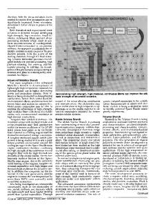
Figure 1. Nucleation of a Ni5AI3 precipitate in the p matrix, viewed along a {111) zone of the matrix.
Local Structure of Materials. The mechanical, chemical, or electrical properties of different materials are determined not only by the crystal structure of the perfect material but also by the defect structure. The conduction properties of Si-based semiconductors are determined by the doping and the defect content; the color of diamonds is governed by the impurities; the strength of ceramics is monitored by the presence of impurity phases. The major research objective of EMAT is to correlate these physical properties to the microstructure of the materials. A typical example is th
Data Loading...