Vacancy Enhanced Boron Activation during Room Temperature Implantation and Low Temperature Annealing
- PDF / 89,032 Bytes
- 6 Pages / 612 x 792 pts (letter) Page_size
- 64 Downloads / 364 Views
Vacancy Enhanced Boron Activation during Room Temperature Implantation and Low Temperature Annealing Jian-Yue Jina, Irene Rusakova, Qinmian Li, Jiarui Liu, and Wei-Kan Chu Physics Department, and Texas Center for Superconductivity, University of Houston, Houston, TX 77204 a)
Present address: Varian Semiconductor Equipment Associates, 35 Dory Road, Gloucester, MA 01930. Electronic mail: [email protected]
ABSTRACT
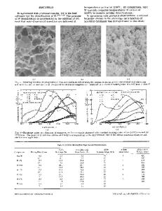
Low temperature annealing combined with pre-damage (or preamorphization) implantation is a very promising method to overcome the activation barrier in ultra-shallow junction formation. We have made a 32 nm p+/n junction with sheet resistance of 290 Ω/sq. using 20 keV 4x10¹⁴ at./cm2 Si followed by 2 keV 1x10¹⁵ at./cm2 B implantation and 10 minutes 550 °C annealing. This paper studies the boron activation mechanism during low temperature annealing. The result shows that placing B profile in the vacancyrich region has much better boron activation than placing B profile in interstitial-rich region or without pre-damage. It also shows that a significant portion of boron is in substitutional positions before annealing. The amount of substitutional boron is correlated to the amount of vacancies (damage) by the pre-damage Si implantation. The result supports our speculation that vacancy enhances boron activation. 1. Introduction The continuous shrinkage of the semiconductor integrated circuits requires fabrication of less than 30 nm ultra-shallow p+/n junctions in the near future.1 Although the present implanter and plasma doping technologies are able to achieve as-implanted boron profile as shallow as 20 nm,2 the post-implant high-temperature annealing process greatly increases the junction depth due to thermal diffusion and the transient enhanced diffusion (TED).3, 4 While reducing annealing temperature usually results in poor boron electrical activation. Consequently, high temperatures (>1000 °C ) rapid thermal annealing (RTA) or spike annealing are preferred to increase boron activation and minimize boron diffusion. Recently, we have fabricated a 32 nm ultra-shallow p+/n junction with sheet resistance of 290 Ω/sq. using combination of pre-damaging implantation and low temperatures annealing.5 The junction parameters overcome the activation barrier for conventional rapid thermal annealing. The pre-damaging implantation was a 20 keV 4×10¹⁴ at./cm2 Si implant, followed with a 2 keV 1×10¹⁵ at./cm2 B implant. The annealing was at 550 ºC for 10 minutes. This work is to study the boron activation mechanism during low temperature annealing. We speculate that there are two steps for boron activation in this low temperature process. The first step is boron moving to the substitutional or quasisubstitutional positions during implantation or at the very beginning of annealing. The second step is damage removing or solid phase epitaxial (SPE) regrowth. The amount of
B5.6.1
1
boron in the substitutional position at the first step should be correlated to the amount of vacancy produced by Si pre-damaging implant. 2. E
Data Loading...