Valence Band Parameters for Wurtzite GaN and InN
- PDF / 425,393 Bytes
- 6 Pages / 414.72 x 648 pts Page_size
- 89 Downloads / 323 Views
(PW,GIJ PSIPWGj) = VS(G, -GJ).Ss(G, -G
j)+iVA
(Gi - Gj ).SA (G, -GJ),
(1)
where IPWG) is a plane-wave state indexed by the reciprocal lattice vector G, VN(G,- Gj) and V4(Gi- Gj) are the symmetric and asymmetric form factors respectively, and Se(Gi- G1) and S4(Gi- Gy) are respectively the symmetric and asymmetric structure factors specific to the WZ 923
Mat. Res. Soc. Symp. Proc. Vol. 482 0 1998 Materials Research Society
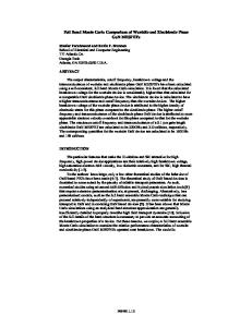
crystal. The basis set of plane waves was chosen with the criterion that IG + kJ lies within a sphere defined by a kinetic energy E1 (= 13.5 Ry). Second order contribution from all vectors G such that IG + kJ lies between the spheres defined by E1 and E2 (= 20 Ry) are also accounted [19]. Initial calculations were performed without considering the spin-orbit (SO) interaction. The form factors in (1) are adjusted to obtain band features at high symmetry points which agree with experimental data and reliable theoretical prediction. These form factors are then used to determine the electronic energy bands on a fine grid of points along the high symmetry lines of the Brillouin zone (BZ) as shown in Fig. 1 for GaN and InN. Details of the adjusted form factors and eigenenergies are documented elsewhere [20]. Convergence tests performed by increasing E1 and E2 showed negligible changes in the eigenenergies. The lattice constants used are a = 3.189 A, c = 5.185 A for GaN, and a = 3.54 A, c = 5.70 A for InN [21]. The internal structural parameter u used for GaN and InN are 0.3768 and 0.3790 respectively [8]. Direct band gaps of 3.50 eV for GaN and 2.04 eV for InN are obtained, in agreement with experimental data [13],[21 ],[23] and elaborate self-consistent calculations with corrections for the LDA error [3]-[5]. The width of the top valence band (arising from N 2p orbitals) for GaN is calculated to be 6.8 eV, near the experimental value of 7.0 eV [24]. For InN, our valence band width of 5.8 eV compares commendably with other calculations: 5.73 eV [11], 5.98 eV [10], and 6 eV [25]. Earlier EPM calculations [16] overestimated the valence band width (9.6 eV). For the crystal-field splitting, Acr, we obtained 21 meV and 17 meV for GaN and InN respectively. InN has a smaller Acr than GaN, in qualitative agreement with Ref. 8 and 9. Our value for Ac, of GaN is consistent with 22 meV as determined by Dingle et al. [26] and the interpretation [27] of recent experimental data [28]. Ac. for InN is not known experimentally. Fine details of the band structure near the F point valence band maximum (VBM) are investigated with the inclusion of the SO interaction. The energies of the top three states, E( F v), E( F() ), and E( r-v(2)), are related to the SO splitting, A,,, and A, by [29] E(F Y)-E(F;")) = [(Ao + Ac,)-
(Aso + Aer) 2 -8AoAc,/3]/2,
E(r;)-E(r.v( 2 )=[(Ao +A")+ (A° +Ar)2 -8AoA, /3]/2.
8
4 3
33
(a)
(b) InN
aN,..2
6 3,63
(2)
6
,
A
Figure 1. The electronic band structure of WZ (a) GaN and (b) InN along the high symmetry lines of the first Brillouin zone calculated by the EPM. Spin-orbit intera
Data Loading...