Reactive Molecular-Beam Epitaxy for Wurtzite GaN
- PDF / 698,381 Bytes
- 7 Pages / 576 x 777.6 pts Page_size
- 104 Downloads / 387 Views
Growth and Characteristics of n-GaN Films Growth To date, a number of growth techniques, such as hydride vapor phase epitaxy (HVPE), metalorganic chemical vapor deposition (MOCVD), and molecular-beam epitaxy (MBE) have been 22
employed to grow III-V nitrides. A variety of substrates, including silicon,11 GaAs,12 silicon carbide,13 and sapphire have been used. Various crystallographic orientations of sapphire14 also have been investigated. Yet until recently, it was difficult to obtain highly resistive undoped GaN films. Native point defects in general and nitrogen vacancies in particular are thought to be primarily responsible for the n-type background of the as-grown films. Threading dislocations and stacking faults are the main structural defects in films, particularly
in between the columns.15 For GaN films grown by RMBE, ammonia (NH3) is used as the active nitrogen source.16 Ammonia is reduced on the surface of the substrate by pyrolysis, allowing AUGai^N ( 0 < I < 1 ) and GaN
to be grown in a temperature range of 700-850°C.17 This growth temperature compares to about 1000°C employed in MOCVD. Although such a growth by RMBE employing NH 3 was tried about a decade ago,18 the RMBE-grown films had poor quality. The only exception was a recent quarter-wave reflector stack growth of AIN-GaN by RMBE,1" which showed over 90"/) of peak reflectance on (100) GaAs. The efforts of Kim et al.20 (KAB) have been very successful. Kim et al. provided NH 3 through an injector maintained at 600°C. The purity of ammonia gas was 99.9995%, which was filtered and purified before being fed into the growth chamber through a mass flow controller to control the ratio of Group V to Group III (hereafter referred to as V/III ratio). The chamber pressure was kept at 2-5 X 10"5 Torr during film growth. Basal plane sapphire and to some extent 6H-SiC were used as substrates. The growth of about 650 A of A1N buffer layer followed by the growth of GaN at a growth temperature of 800°C was then successfully performed.
50
600
650
700
750
800
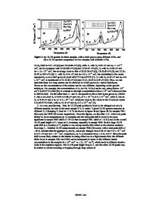
Substrate Temperature (°C) Figure 1. Variation of x-ray rocking curve full width half maximum (FWHM) with substrate temperature (ammonia flow rate = 16 seem).
MRS BULLETIN/FEBRUARY 1997
Reactive Molecular-Beam Epitaxy for Wurtzite GaN
Characteristics ofn-GaN The KAB films were characterized by x-ray diffraction (XRD) 9-26 scan, and double crystal triple axis w-scan using Cu-Ka and Mo-Ka lines, respectively. While the optical properties were characterized by photoluminescence (PL) spectroscopy using 325 nm excitation produced by a He-Cd laser, the electrical properties were measured by the Hall measurement using the van der Pauw configuration. Ti/Al/Ti or Ti/Al/Ni/Au metallization, which involved rapid thermal annealing (RTA) at 900°C for 30 s, was used for ohmic contacts. Structural Characteristics. Out-ofplane and in-plane XRD investigations were carried out. The out of plane XRD rocking curve exhibited a full width half maximum (FWHM) of about 4.7 min. This was comparable to that of Nakamura21 et
Data Loading...


