X-Ray Study of Strained and Strain Balanced Superlattice Materials
- PDF / 338,685 Bytes
- 4 Pages / 432 x 648 pts Page_size
- 61 Downloads / 419 Views
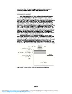
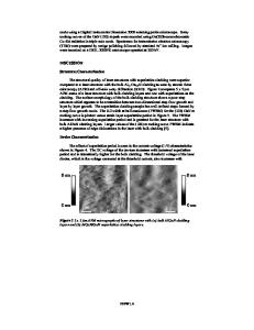
X-Ray Study of Strained and Strain Balanced Superlattice Materials Natee Johnson1, Ruth Choa3, Liwei Cheng2, Fow-Sen Choa2 1 Mechanical Engineering, University of Maryland, Baltimore County, Baltimore, MD, USA. 2 Computer Science and Electrical Engineering, University of Maryland, Baltimore County, Baltimore, MD, USA. 3 School of Engineering and Applied Science, Harvard University, Cambridge, MA, USA. ABSTRACT Nano-scale superlattice (SL) based devices, such as quantum cascade lasers QCLs, have recently become very important due to their capability to identify toxic and explosive chemicals. In manufacturing these Mid-IR photonic devices, atomic-level scanning tunneling microscopes (STM) and transmission electron microscopes (TEM) have been used to characterize the growth quality of superlattice wafers. However, these methods yield observations that are localized and cannot view the entire structure and even now we have not been able to correlate these measured crystal lattice images with device performance. The x-ray scanning technique has greater likelihood of success given that it can observe not only the localized, but also the entire superlattice structure. By extracting special features and key parameters in x-ray diffraction (XRD) patterns, the epitaxial quality of QCL superlattices can be evaluated and correlated to the performance of fabricated QCL devices. We can then differentiate and classify different grades of wafers before starting device fabrication and testing. Such an example of the usefulness of XRD can be found with strain-balanced superlattices, such as InGaAs/InAlAs, where there is notable decrease in laser performance after relaxation. It can also be found with type-II InAs/GaSb strained layer superlattice, which is currently the best candidate for room temperature mid-IR detectors and focal plane arrays. Experimentally measured x-ray patterns are compared to simulation results and problem sources are identified. INTRODUCTION Nano-scale SL based devices such as quantum well infrared photodetectors (QWIPs) and QCLs have existed for more than a decade. However, even now, we still lack of a systematic methodology to study and understand the relationship between material quality and device performance. For example, interface and surface states affect interband devices significantly because their carrier lifetime is in the nanosecond to microsecond scale. On the other hand, it is not clear how hetero-interface states affect the performance of intersubband devices because their lifetime (intersubband state) is in the picosecond to sub-picosecond level. Furthermore, a typical 30-period QCL can easily have >1000 slices of nano-scale-thick layers with a total thickness of a few microns. The analyzing method needs to be able to simultaneously examine the quality of all the layers in each one of the 30 periods. The diffraction of an x-ray through a superlattice material is a Fourier transformation of the superlattice structure (in x-space) to the k-space, expressed by the profile of diffraction angles, wh
Data Loading...