ZnO Field-Effect Transistors Fabricated on Self-Assembled Colloidal Nanorods
- PDF / 138,090 Bytes
- 1 Pages / 612 x 792 pts (letter) Page_size
- 48 Downloads / 325 Views
(p. G367), ultrathin (< 5 nm) HfO2 films were grown using atomic layer deposition on 12-in. p-type silicon (100) substrates. Xenon FLA was then conducted at capacitor charging voltages of 3100–3500 V with a 0.8-ms pulse width. The samples were preheated to 400ºC in a N2 atmosphere. Xray diffraction (XRD) measurements were performed on the samples subjected to xenon FLA and conventional rapid thermal annealing. TaSi2.5 (10 nm)/ W (100 nm) gate electrodes were then sputter-deposited for capacitance–voltage (C–V) and current– voltage (I–V) measurements. According to Kamiyama and co-workers, the actual wafer temperature during FLA is not known. XRD measurements on HfO2 films after rapid thermal annealing suggest that the crystallization temperature of HfO2 films is ~600ºC. The onset of post-FLA crystallization for similar films begins at capacitor charging voltages of 3300 V. C–V and I–V measurements on HfO2 gate dielectrics with TaSi2.5/W gate electrodes after xenon FLA show an increase in dielectric constant, and leakage current values comparable with similar samples after annealing in O3. Although the films show a slight decrease in equivalent oxide thickness (~5%) after FLA, the researchers said this process shows promise for manufacturing high-κ–based transistors with metal gates. JEREMIAH T. ABIADE
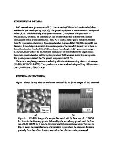
ZnO Field-Effect Transistors Fabricated on Self-Assembled Colloidal Nanorods Zinc oxide (ZnO) is a transparent semiconductor with a large bandgap. ZnO thinfilm field-effect transistor (TFT) devices fabricated with colloidal ZnO nanocrystals are particularly attractive because they are based on a low-temperature, solutionprocessible semiconducting material. Researchers Baoquan Sun and Henning Sirringhaus of the University of Cambridge have now fabricated high-performance ZnO TFT devices on a SiO2/Si substrate by spin-coating an aqueous suspension of ZnO nanocrystals to form a thin film on the substrate. As reported in the December 2005 issue of Nano Letters (DOI: 10.1021/nl051586w; p. 2408), the researchers investigated the effects of the nanocrystal shape on the colloidal self-assembly of the nanoparticles on the substrate and on the resulting device performance. They found that by changing the shape of the nanocrystals from sphere to rod, the semiconducting properties of the spin-coated ZnO films were greatly improved as the result of increased particle size and self-alignment along the substrate. Post-deposition hydrothermal growth of the nanorods in an aqueous zinc-ion solution was found to further enhance the nanorod dimensions and interconnectivity and significantly
more research on For For more research newsnews on Materials Science, access the Science, Materials Research Society Materials Web site: access the Materials Research Society Web site: www.mrs.org/connections www.mrs.org/connections
Journal of Materials Research (JMR)
MRS Bulletin timely insight into the current status and trends in materials research
because important work deserves to be published quickly
www.mrs.org/bulletin/ 84
improve the de
Data Loading...