A Chemical Approach to 3-D Lithographic Patterning of Si and Ge Nanocrystals
- PDF / 385,692 Bytes
- 6 Pages / 612 x 792 pts (letter) Page_size
- 40 Downloads / 266 Views
0901-Rb09-03.1
A Chemical Approach to 3-D Lithographic Patterning of Si and Ge Nanocrystals I.D. Sharp,a,b Q. Xu,a,b D.O. Yi,a,c C.Y. Liao,a,b J.W. Ager III,a J.W. Beeman,a K.M. Yu,a J.T. Robinson,a,b O.D. Dubón,a,b D.C. Chrzan,a,b and E.E. Hallera,b a)
Materials Sciences Division, Lawrence Berkeley National Laboratory, Berkeley, CA 94720 Materials Science and Engineering Department, University of California, Berkeley, Berkeley, CA 94720 c) Applied Science and Technology Group, University of California, Berkeley, Berkeley CA 94720 b)
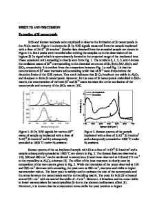
ABSTRACT Ion implantation into silica followed by thermal annealing is an established growth method for Si and Ge nanocrystals. We demonstrate that growth of Group IV semiconductor nanocrystals can be suppressed by co-implantation of oxygen prior to annealing. For Si nanocrystals, at low Si/O dose ratios, oxygen co-implantation leads to a reduction of the average nanocrystal size and a blue-shift of the photoluminescence emission energy. For both Si and Ge nanocrystals, at larger Si/O or Ge/O dose ratios, the implanted specie is oxidized and nanocrystals do not form. This chemical deactivation was utilized to achieve patterned growth of Si and Ge nanocrystals. Si was implanted into a thin SiO2 film on a Si substrate followed by oxygen implantation through an electron beam lithographically defined stencil mask. Thermal annealing of the co-implanted structure yields two-dimensionally patterned growth of Si nanocrystals under the masked regions. We applied a previously developed process to obtain exposed nanocrystals by selective HF etching of the silica matrix to these patterned structures. Atomic force microscopy (AFM) of etched structures revealed that exposed nanocrystals are not laterally displaced from their original positions during the etching process. Therefore, this process provides a means of achieving patterned structures of exposed nanocrystals. The possibilities for scaling this chemical-based lithography process to smaller features and for extending it to 3-D patterning is discussed. INTRODUCTION The ability to precisely control nanocrystal growth sites and/or their placement is of critical importance for realization of functional nanocrystal-based devices, for single and ensemble nanocrystal measurements, and possibly for additional control of nanocrystal sizes. Patterning of solution-processed nanocrystals has been achieved by a number of techniques.[1-6] However, production of colloidal Group IV semiconductor nanocrystals is difficult and it is often preferable to form them within a solid matrix, usually SiO2. While patterned growth of embedded nanocrystals has been realized, only a limited number of techniques have been explored thus far.[7-10] Here, we demonstrate the patterned growth of ion beam synthesized Si and Ge nanocrystals. Chemical deactivation of the nucleating specie is achieved by coimplantation of oxygen through a lithographically defined mask. Furthermore, we show that by varying the oxygen dose, the light emission energy of Si nanocrystals may be tuned
Data Loading...