A Comparative Study on Electromigration Failure Mechanism Between Near-Bamboo and Bamboo Al(Cu) Two-Level Structure
- PDF / 1,979,860 Bytes
- 6 Pages / 414.72 x 648 pts Page_size
- 42 Downloads / 372 Views
ABSTRACT
As the interconnect line width reduces to the sub-micron range, the grain distribution of AI(Cu) alloy lines reaches a bamboo structure. Understanding of the electromigration resistance of near-bamboo and bamboo structures is essential to the sub-micron reliability issue. In this study, the mass transport and failure mechanism of 1 gm wide Al(1%Cu) two-level lines with near-bamboo and bamboo structures were investigated by a drift velocity technique [1]. Our results show that interfacial (AIOx/Al interface) diffusion coupled with grain boundary diffusion determines the failure mechanism of bamboo lines.
INTRODUCTION
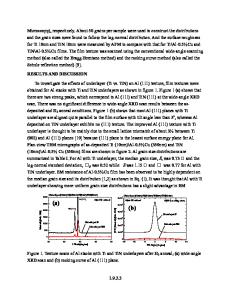
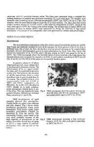
It is known that electromigration failure is strongly related to the metal line microstructure. The grain distribution of Al(Cu) alloy lines reaches a bamboo structure as the interconnect line width reduces to the sub-micron range. In addition, an increased median lifetime t5 0 was reported as the microstructure of sub-micron lines becomes bamboo-like [2]. Several failure mechanisms has been proposed to explain this phenomena, including the interfacial [3] and lattice [4] diffusion. The electromigration failure mechanism is still not very consistent for interconnects with sub-micron linewidths. Therefore, the objective of this study is to understand the electromigration failure mechanism of 1 gm wide Al(l% Cu) two-level lines with near-bamboo and bamboo structures. In this study, the failure mechanism of 1 gim wide AI(I%Cu) two-level lines with nearbamboo and bamboo structures were investigated. These two grain structures were attained by using different substrate temperature during the AI(1%Cu) sputtering process. The drift velocity method is applied to investigate electromigration in this study because this method allows us to directly observe the damage formation process. Scanning electron microscopy (SEM) was used to observe the void formation process in near-bamboo and bamboo structures by interrupting the current stressing conditions at preset time intervals. Focused ion beam (FIB) microscopy was employed to understand the grain structure around the voids formed after the test. 265
Mat. Res. Soc. Symp. Proc. Vol. 391 01995 Materials Research Society
EXPERIMENTAL
The two-level structure used in this study is a line/plug/line configuration or M 1-W-M2 structure, where Ml, W, M2 are the first level metal lines, tungsten plugs and second level metal lines, respectively. All the test structure were processed on thermally oxided 5 inch silicon (100) wafers. The MI layers of Ti(200 A)/TiN(600 A)/Al(l% Cu)(6000 A)/TiN(250 A) were deposited sequentially onto the oxided silicon wafers by direct current (DC) magnetron sputtering. Standard ultraviolet (UV) photolithography and reactive ion etch (RIE) techniques were used to pattern the lines. The M1 line length was chosen to be 5 jim which is shorter than the critical line length. Therefore, no electromigration mass transport occurs on the first level metal lines. After patterning the MI lines, a 4000 A tetraethylorthosilicate (TEOS) film was
Data Loading...