A New Low Dielectric Constant Polymer Material (k < 2): Microstructure, Electrical Properties, and Mechanical Propert
- PDF / 1,573,363 Bytes
- 6 Pages / 417.6 x 639 pts Page_size
- 6 Downloads / 334 Views
17 Mat. Res. Soc. Symp. Proc. Vol. 565 ©1999 Materials Research Society
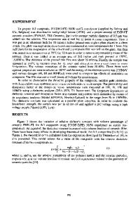
Ta metal layer. The thickness of the Au and polymer films could then be measured by an alpha-step technique, by ellipsometry, or by cross-sectional Scanning Electron Microscopy (SEM). To make a porous PAE film, a modified PAE solution was made by adding a certain amount of a specially prepared organic solution. The mixture of these two solutions was stirred at room temperature and set aside for one day for aging. The porous film was then prepared by the same procedure as the dense PAE film mentioned above, except that the curing was done in air. Electrical Properties The dielectric constant was measured by using fabricated MIM (Metal-InsulatorMetal) structures. The Ta layer was used for the lower electrode and the sputtered Au dots with a diameter of 0.18cm were used for the upper electrode. The lower electrode was exposed by dry etching technique or pre-exposed method. The capacitance (C) and dissipation factor (D) of the ILD thin films were measured by using an HP 4192A impedance analyzer with frequency of IMHz and voltage 0. IV. Leakage current was measured from the test wafers with single metal layer interconnect structures. The metal stack of Ti(500A)/Al-Cu:0.5%(6000A)/TiN (250A) was patterned on a Si0 2 (10000A) layer on a Si substrate. The 0.3iim spaced comb/serpentine metal structure was selected for testing. Both dense and porous PAE dielectric films were spin-coated on the test wafers and cured using the process conditions mentioned before. For leakage current measurements, the measurement probes were pushed to penetrate the polymer film on the pads and voltage was swept between OV and 70V. The leakage current from the metal lines was obtained from a current meter (Keithley 617). Microstructure and Gapfilling High Resolution Transmission Electron Microscopy (HRTEM) was used to investigate the microstructure difference between dense and porous films. The crosssection HRTEM pictures were taken from the samples with low-k thin films coated on a Ta/Si substrate. High Resolution Scanning Electron Microscope (HRSEM) was used to look at the gapfilling properties of the dense and porous films. HRSEM photographs were taken at 0.3 pim space between the metal lines. Thermal Cycling Thermal stress of the low-k ILD thin films (both dense and porous) was measured by a Flexus system. The dielectric thin films were spin-coated on a 4-in bare Si substrate. The dense PAE films were heated to 400'C under N2 ambient, while porous PAE films were heated to 350'C in air. The ramping rates for the heating and cooling process were controlled at 1.5C /min. Both types of samples were kept in the highest temperature for half an hour. The initial and in-situ stress was calculated from the curvature change. Il. RESULTS The dielectric constant of a two-phase solid-gas mixture material can be calculated by [11] lnk,= vi lnkl+v 2 Ink 2 (1)
18
N
3.2
332
I
A A
228
A,DenseA
A
PAE
2.8
A
2.4
C
24
0
S20 0
2.0
S1.6 ýI
Porous PAE
1.6
U
_ 12
1,2
o
Data Loading...