A New Method for the Simultaneous Analysis of I-V/T and C-V/T Measurements of an Au/P-Inp Epitaxial Schottky Diode
- PDF / 346,971 Bytes
- 6 Pages / 414.72 x 648 pts Page_size
- 43 Downloads / 247 Views
P. COVA*, A. SINGH*, R. A. MASUT** and J. F. CURRIE** Universidad de Oriente, Departamento de Ffsica, Laboratorio de Modelaje de Dispositivos Semiconductores, Apartado 188, Cumand 6101, Sucre, Venezuela. Ecole Polytechnique de Montreal, Ddpartement de g6nie physique, C.P. 6079, Succ. "Centre-Ville", Montreal (Quebec) H3C 3A7, Canada.
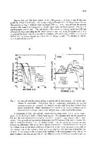
ABSTRACT We have developed a new approach to analyze the current- voltage (I-V) characteristics of a tunnel metal-interface layer - semiconductor (MIS) diode which takes into account the voltage dependence of interface states distribution (N,) and the barrier lowering due to image force. Our method of analysis uses simultaneously the I-V/T and C-V/T data to determine the characteristic parameters of an MIS diodes and is ideal for new epitaxial materials and devices where the carrier density is not known precisely before hand. The experimental verification of our approach to analyze the nonideal I-V/T and C-V/T characteristics of MIS diodes was done by comparing the values of N,, extracted from the room temperature forward I-V characteristics of a p-InP/Au MIS diodes with those obtained by the multi-frequency admittance method. Excellent agreement between the values of N, determined by two different techniques strongly support the validity of our theoretical expression for the I-V/T characteristics and the method of analysis. Our results indicate that the interface layer thermionic emission was clearly the dominant mechanism of the forward current transport in epitaxial Au/p-InP MIS diodes over the temperature range 200-393 K. The transmission coefficient of the interface-layer obtained from the reverse I-V characteristics has a value of 1.43x I0W (±_7%). INTRODUCTION The physics of MIS diode has been discussed in many papers [1-13] and a lot of attention has been drawn to the characterization of the MIS diodes [1,10-13]. In spite of the experimental evidence of voltage dependence of the interface states distribution [1, 10-12], many authors assume a constant interface states density distribution in the analysis of the I-V characteristics [8-9, 13]. Some authors have used both the I-V/T and C-V/T characteristics simultaneously to determine the relevant parameters of the MIS diodes [1,12]. In this paper, we present a formalism to treat the nonideal I-V characteristics of an MIS diode taking into account a voltage dependent interface states distribution and the barrier lowering due to the image force. Using this formalism, we have developed a new method to analyze simultaneously the I-V/T and CV/T data of an MIS diode to determine its characteristic parameters. This analysis has been applied to examine the current transport mechanisms in an epitaxial p-InP/Au MIS diode. THEORETICAL BACKGROUND For an MIS structure with interface states, the equivalent circuit depends on the occupancy function of the interface states (f0 ). When f,,, is controlled by the occupancy function of the interface states in equilibrium with the metal (tf,), the interface states capacitance (C ) is in parallel with
Data Loading...