Parameter Extraction from the Reverse I-V and C-V Characteristics of an Epitaxial p-InP/Au Schottky Diode
- PDF / 342,906 Bytes
- 6 Pages / 414.72 x 648 pts Page_size
- 53 Downloads / 379 Views
Universidad de Oriente, Departamento de Ffsica, Laboratorio de semiconductores, Apartado 188, Cumand 6101, Sucre, Venezuela 1,cole Polytechnique de Montr6al, Ddpartement de genie physique, C.P. 6079, Station "Centre-Ville", Montrdal (Quebec), H3C 3A7, Canada
ABSTRACT
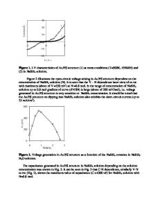
Epitaxial p-InP/Au Schottky diodes were fabricated by evaporation of Au onto Zn doped epitaxial layers of InP grown by MOVPE, on a highly doped InP substrate. The reverse currentvoltage (I,-V,) and 1 MHz capacitance-voltage (C-V) characteristics of the Au/p-InP diodes were measured in the temperature range 220-393 K. At all temperatures, soft reverse current-voltage characteristics were observed, which may be due to the decrease in the effective Schottky barrier height (0br) with the increase of Vr. The voltage dependence of the reverse current was well described in terms of the interface layer thermionic emission (ITE) model which incorporates the effects of applied reverse voltage drop and the transmission coefficient across the interface layer and image force lowering of the barrier height into the thermionic emission theory. A self consistent iteration and least square fitting technique was used to obtain the zero bias barrier height (0b.) and interface layer capacitance (Ci) from the Ir-V, data. Both, the 4r-V, and the C-V data were analyzed under the assumption of reverse bias voltage independence of the charge trapped in the interface states, which was supported by our experimental data. The values of dbo obtained from the C-V measurements agreed well with those obtained from the I1-V, data for a value of 0.45 AK 2cm2 for the effective Richardson constant (Aeff). INTRODUCTION
InP is a promising material for the manufacture of solar cells, high speed FETs,
optoelectronic and microwave devices. Fabrication of good quality metal- semiconductor (MS) and metal-thin interface layer-semiconductor (MIS) junctions and the knowledge of their characteristic parameters is vital to the efficient operation of the InP-based devices such as high speed FETs and MIS solar cells. The Schottky barrier height is one of the most important parameter of the MS and MIS devices because it controls both the current-voltage (I-V) and the capacitance-voltage (C-V) characteristics. Therefore, to determine its correct value, both the I-V and the C-V data at different temperatures (T) should be analyzed simultaneously. Some authors have used the C-V/T and the forward I-V/T measurements to obtain the characteristic parameters of the Schottky type contacts to bulk p- InP semiconductor [1,2]. However, to the best of our knowledge, the estimation of the characteristic parameters of Schottky type contacts to epitaxial p-InP layers from the reverse current-current-voltage/temperature (I-V,/T) and C-Vr/T characteristics has not been carried out. In. this work, we present the temperature variation of the I,-Vr and 1 MHz C-Vr/T characteristics for an epitaxial p-InP/Au Schottky type diode and report a method to extract the diode's parameters from these measurements.
135 Mat. Res.
Data Loading...