Diamond Schottky Barrier Diode with Fluorine- and Oxygen-Termination
- PDF / 543,990 Bytes
- 7 Pages / 432 x 648 pts Page_size
- 71 Downloads / 358 Views
Advances:
Email alerts: Click here Subscriptions: Click here Commercial reprints: Click here Terms of use : Click here
Diamond Schottky Barrier Diode with Fluorine- and OxygenTermination Chao Hu, Zhangcheng Liu, Jingwen Zhang, Wei Wang and Hong-Xing Wang MRS Advances / Volume 1 / Issue 16 / January 2016, pp 1125 - 1130 DOI: 10.1557/adv.2016.135, Published online: 15 February 2016
Link to this article: http://journals.cambridge.org/abstract_S2059852116001353 How to cite this article: Chao Hu, Zhangcheng Liu, Jingwen Zhang, Wei Wang and Hong-Xing Wang (2016). Diamond Schottky Barrier Diode with Fluorine- and Oxygen-Termination. MRS Advances, 1, pp 1125-1130 doi:10.1557/adv.2016.135 Request Permissions : Click here
Downloaded from http://journals.cambridge.org/ADV, IP address: 207.162.240.147 on 26 Aug 2016
MRS Advances © 2016 Materials Research Society DOI: 10.1557/adv.2016.135
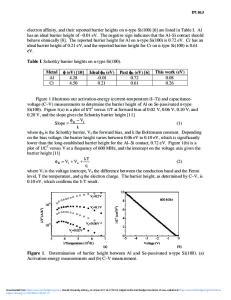
Diamond Schottky Barrier Diode with Fluorine- and Oxygen-Termination Chao Hu, Zhangcheng Liu, Jingwen Zhang, Wei Wang, Hong-Xing Wang Institute of wide band gap semiconductors, Xi'an Jiaotong University, Xi'an, China. ABSTRACT Schottky properties of Mo on diamond with fluorine- and oxygen-termination had been investigated. Oxygen-termination was generated by aqua regia. Fluorine-termination was generated by CF4 plasma treatment. Mo/Ni/Au was deposited on the diamond surface as Schottky electrode, whose barrier height was evaluated from current-voltage curve. After that, the X-ray photoelectron spectroscopy methods were applied to calculate the Schottky barrier height of Mo on different termination surface. The results indicated that the fluorine-termination and oxygen-termination show different schottky properties. INTRODUCTION Diamond has outstanding properties, such as a wide band gap (5.5 eV), high breakdown field (10 MV/cm), high thermal conductivity (22 W/(cm•K)), and high hole and electron mobility (3800 cm2/V•s and 4500 cm2/V•s), which making it a promising semiconductor for realization of high power and high frequency devices. This has encouraged researchers to extensively investigate diamond semiconductor fabrication technologies, such as high quality diamond film growth, diamond n- and p-type doping, device designing, etc. However, it is hard for diamond to efficiently generate carriers at room temperature by conventional impurity doping methods because of the high activation energy, such as 0.37 eV for boron and 0.6 eV for phosphorus. Fortunately, there is a unique way for diamond to generate carriers. When diamond is terminated by hydrogen, with an adsorbate layer, it generates two-dimensional holes gas (2DHG) at the surface, whose carrier density is higher than 1E13 cm-2 [1]. Furthermore, the hydrogenterminated diamond exhibits negative electron affinity with the value of -1.3eV [2, 3]. On the contrary, diamond surface also can be terminated by oxygen which shows positive electron affinity [4]. That means, metal contact on hydrogen-terminated diamond and oxygen-terminated diamond will show different properties, which illust
Data Loading...


