A New Way to Form Three-Dimensional Microstructures by Electrochemical Etching of Silicon
- PDF / 192,833 Bytes
- 6 Pages / 612 x 792 pts (letter) Page_size
- 10 Downloads / 236 Views
A New Way to Form Three-Dimensional Microstructures by Electrochemical Etching of Silicon P. Kleimann1, J. Linnros and R. Juhasz Department of Electronics, Kungl. Tekniska Högskolan, Electrum 229, S-164 40 Kista, SWEDEN 1 LENAC, Université Claude Bernard Lyon-I, 43 Bd. du 11 Novembre 1918, 69622 Villeurbanne, France
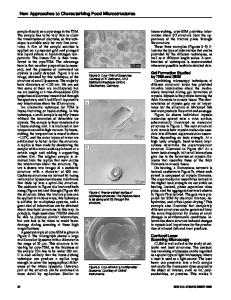
ABSTRACT A new technique of bulk micromachining using anodic etching of (100)-oriented n-type silicon is presented. For particular conditions the transition regime between porous silicon formation and electropolishing enables the formation of high aspect ratio microtips which correspond to inverted macropore structures. This unusual property can be explained by the distortion of current lines near the basis of formed structures. The distortion, which prevents the tip dissolution, is due to the electrical field in the space charge region at the silicon-electrolyte interface. The same property can be used to form three-dimensional microstructures. The position and shape of the structures can be defined by forming steps of a few microns depth, prior to the electrochemical etching. Then the etching parameters (HF concentration, light intensity, etching current density) are adjusted in order to electropolish the sample except where vertical walls are needed. This enables to form microstructures without a periodic pattern. The feasibility of this technique is demonstrated by forming 100 µm wide pores, free-standing beams as well as high aspect ratio micro-needles and micro-tubes. INTRODUCTION Anodic dissolution of silicon is, for four decades [1], well known as a technique of porous silicon formation or electropolishing. This technique has recently emerged in bulk micromachining due to its ability to form high aspect ratio macropores or trenches in n-type silicon substrates [2]. Basically the technique consists in forming a regular array of pores or trenches, which serve as frames to form microstructures [3,4]. Here, we present a new way to form high aspect ratio and free-standing structures without a necessary spatial periodicity. This technique is also based on anodic etching of (100)-oriented ntype silicon and involves the property of the transition regime. This regime enables electropolishing of the surface except where vertical walls or pillars are needed. Proof of principle experiments have been carried out by forming 100 µm wide pores, free standing beams, high aspect ratio micro-needles and micro-tubes.
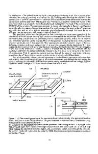
BASIC PRINCPLE Depending on etch current density, anodic dissolution of silicon in hydrofluoric acid can be divided into three different regimes: For etching current densities well below a critical value, F8.2.1
often called Jps, anodic dissolution leads to the formation of porous silicon. Above this value, electropolishing occurs [5,6]. Now, as shown in figure 1, for specific conditions the transition regime between porous silicon formation and electropolishing can be reached enabling the formation of microtips. Such unusual regime is observed in the case of n-type silicon anodization, when minorit
Data Loading...