In Situ Observation of an Electrochemical Etching Reaction in Silicon
- PDF / 3,648,693 Bytes
- 6 Pages / 414.72 x 648 pts Page_size
- 96 Downloads / 324 Views
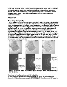
by making use of the selectivity of the etching process to the Si doping level. For a given applied potential, the order of reactivity is n+>p+>p->n- [5]. Etching could therefore be confined to the central layer of an MBE-grown n-/n+/n- sandwich with a suitable etch rate differential between the central layer and the outer ones. The reaction was observed in an electron transparent region of the specimen which was created by (non-electrochemical) etching from the back of the wafer with an HF/HNO 3/HAc solution. The specimen geometry is shown schematically in figure 1, and figure 2 shows the selective nature of the etching reaction. The confinement of the pores to the n+ layer was very effective and we were able to propagate pores horizontally through this layer by up to 1500gm, creating structures with an aspect ratio of about 104. The specimen holder must be designed so that electrolyte can come into contact with the specimen but can not escape into the high vacuum environment of the microscope. This is achieved by constructing a small reservoir, 3x4x6mm, from a machinable ceramic, with a slot in one end into which the specimen can be inserted. Most of the specimen (including the electron transparent window) protrudes out of the reservoir. The specimen is painted around its edges with wax, defining a window on the top surface which is to come in contact with the electrolyte. It is then sealed into the reservoir with epoxy and the reservoir is filled with electrolyte (49% HF) through a screw hole in the other end. Finally, a screw is inserted into the hole; this extends into the electrolyte and forms the negative electrode. Contact to the Si is made via silver paint at the far end of the specimen. With this geometry, current must pass through the upper n- layer twice on its way to and from the n+ layer, but this is not a problem as the n- layer is only 200nm thick. The whole assembly of reservoir and specimen is clamped into a specimen rod compatible with a JEOL 200CX microscope (figure 3). Electrical connections pass through the rod, linking the positive and negative electrodes to a Fischione power supply operated at constant voltage. Typical conditions were a voltage of 1-3V and a total current flow of 0.01 mA. (a)
HF
area of contact wihelectrolyte
VACUUM electron transparen ,/ window/
Ag paint /Apat
-
025mm
wax
WSS~
mm•
wax
wall of reservoir
A
i
t
n
i'-currentflo (b)
HF
P-N SiO: 2
LLZ;_si// Figure 1. (a) The overall geometry of the specimen shown schematically. The specimen is cut so that its long axis is in the [100] direction. The pore front can be observed once it reaches the long, rectangular electron transparent region. (b) Details of the multilayered structure of the specimen. The starting material is a p-type wafer with a buried oxide layer capped with single crystal silicon. The oxide layer acts as an etch stop when forming the electron transparent region, and also prevents current flow through the substrate. An n-/n+/n- sandwich is grown on the wafer by MBE. Electrochemical pore forma
Data Loading...