Etching Silicon Through an Effective Nanomask: An Electrochemical Way to Nanomachining
- PDF / 334,685 Bytes
- 6 Pages / 612 x 792 pts (letter) Page_size
- 86 Downloads / 281 Views
J13.9.1
Etching silicon through an effective nanomask: an electrochemical way to nanomachining
Stefano Borini*, Andrea M. Rossi, Luca Boarino, Giampiero Amato Nanotechnology and Microsystems Dept., IEN Galileo Ferraris, Strada delle Cacce 91, 10135 Torino, Italy * Corresponding author, E-mail: [email protected]
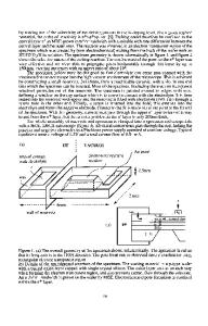
ABSTRACT We present a novel approach to silicon nanomachining, based on the electrochemical etching of the material through a nanopatterned mask.Combining a porous silicon (PS) buffer layer with cross-linked poly(methyl methacrylate) (PMMA) we have obtained masks which show high resistance to the electrochemical etching. PMMA is normally dissolved in a HF/EtOH mixture, but it becomes resistant to such a solution after cross-linking of the polymer. This can be achieved by high-dose electron irradiation in a Scanning Electron Microscope (SEM), obtaining a mask for the subsequent etching. Anyway, due to the strong electric field across the masking layer during the electrochemical process, time duration of such a mask is limited. We demonstrate that the presence of a highly porous silicon thin film lying under the resist leads to an evident improvement of the masking power. A final PS removal leads to the formation of silicon micro- and nanostructures in relief, such as microtips and nanomolds. Thus, we have at hand a simple silicon nanomachining process, where the nanofeatures written by the electron beam in the SEM are transferred to the bulk material through a short anodization step in acid solution. This may be a useful alternative method for fabricating nanodevice elements, such as nanofluidic channels or field emitter arrays.
INTRODUCTION The fabrication of Nano-Electro-Mechanical Systems (NEMS) and nanodevices requires the ability of nanostructuring bulk materials in a controlled and flexible manner. Thus, lithographic methods have to be coupled to etching processes in a convenient way, to get highresolution machining of the substrates. We have explored the possibility of nanomachining silicon wafers by means of two well-assessed techniques, Electron Beam Lithography (EBL) and electrochemical etching, in order to find a new and technologically easy nanofabrication process. Much interest in silicon electrochemistry was attracted in the last 15 years by the discovery of some peculiar properties, such as photo- and electroluminescence [1,2], of Porous Silicon (PS), obtained by Si anodization in HF solution. Moreover, many approaches have been proposed to achieve PS patterning for new devices fabrication. In this respect, some nonstandard techniques, e.g. photolithographic electrochemical process [3] and resistless nanolithography [4], have been reported. Anyway, the typical approach consists in etching silicon through a pre-patterned mask, which must withstand the aggressive HF-based solution.
J13.9.2
To this aim, various masking layers have been proposed, such as Au [5], photoresist [5,6], silicon oxide [7], silicon carbide [6] and silicon nitride [5]. In the present paper, we show that the combination of
Data Loading...