A Novel Back-Reflecting UV-Assisted Metal-Induced Crystallization of Silicon on Glass
- PDF / 480,914 Bytes
- 6 Pages / 612 x 792 pts (letter) Page_size
- 1 Downloads / 208 Views
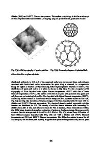
A Novel Back-Reflecting UV-Assisted Metal-Induced Crystallization of Silicon on Glass Leila Rezaee, Shamsoddin Mohajerzadeh, Ali Khakifirooz*, Saber Haji, Ebrahim Asl Soleimani Electrical and Computer Eng. Dept., University of Tehran, Tehran 14395-515, IRAN. * Currently at Department of Electrical Engineering and Computer Science, Massachusetts Institute of Technology, Cambridge, MA 02139, U.S.A. [email protected]. ABSTRACT A novel method of UV-assisted metal-induced-crystallization is introduced to grow polysilicon films on ordinary glass at temperatures as low as 400°C. Annealing is accomplished in the presence of an ultra-violet exposure, leading to high crystallinity of the silicon film as confirmed by XRD, TEM and SEM analyses. A back-reflecting chromium layer is incorporated to further trap UV photons and enhance their absorption in the silicon film. This results in a significant increase in the crystallization rate as studied by XRD spectroscopy. A growth rate of 2 µm/hr is observed at 400°C, when employing this method for lateral crystallization. Thin-film transistors fabricated using the proposed UV-assisted MILC show a threshold voltage of 1V and hole mobility of about 50 cm2/V.s. INTRODUCTION Low temperature crystallization of a-Si is an important objective in fabricating highperformance low cost devices for large-area applications. Excimer laser annealing (ELA) and solid-phase crystallization (SPC) are conventionally used to obtain polycrystalline silicon [1-3]. Although ELA is a fast and low temperature crystallization technique, it is rather complex and expensive. On the other hand, SPC is an energy-consuming and slow technique, which cannot be used at temperatures below 550oC. However, the processing temperatures should be lowered to 450oC to allow using low-cost ordinary glass substrates [4]. Metal-induced crystallization (MIC) is a newly developed method, in which the incorporation of metal facilitates the crystallization of silicon [5-8]. High-performance thin-film transistors have been successfully fabricated using a metal-induced lateral crystallization method [9-13]. However, the processing temperature of 500°C, reported so far for nickel-induced crystallization is still beyond the softening temperature of ordinary glass. Recently we have developed a novel UV-assisted MIC technique, in which some of the energy required for the crystallization is imparted from energetic UV photons [14]. Nickelinduced crystallization of a-Si has been performed at a temperature of 400°C and at the presence of a UV exposure. In this paper a new method is introduced in which a back-reflecting layer is employed to further trap the UV photons and enhance their absorption in the silicon layer. EXPERIMENTAL Fabrication of the samples starts with sputter deposition of a chromium layer with a thickness of 2000Å on 150µm-thick ordinary glass, followed by 1000Å of silicon nitride to isolate Cr and the subsequent Si layer. The a-Si layer, with a thickness of 1500Å is deposited at a temperature of 400oC using electron beam eva
Data Loading...