Numerical Modeling of High Repetition Rate Pulsed Laser Crystallization of Silicon Films on Glass
- PDF / 163,441 Bytes
- 6 Pages / 612 x 792 pts (letter) Page_size
- 18 Downloads / 352 Views
Numerical Modeling of High Repetition Rate Pulsed Laser Crystallization of Silicon Films on Glass
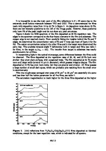
Jürgen R. Köhler, Ralf Dassow, and Jürgen H. Werner Universität Stuttgart, Institut für Physikalische Elektronik, Pfaffenwaldring 47, D-70569 Stuttgart, Germany, [email protected] ABSTRACT This contribution investigates the crystallization behavior of amorphous silicon films on glass by using pulsed lasers with very high repetition rates up to 100 kHz. We determine the influence of the laser repetition rate f and of the film thickness d on the grain width g of the resulting polycrystalline silicon films. Our experimental results indicate a strong dependence of the grain width g on film thickness d as well as on the repetition rate f of the laser. The grain width rises from g = 0.27 µm to g = 3.59 µm if the film thickness increases from d = 50 nm to d = 300 nm and the repetition rate f from f = 20 kHz to 100 kHz. We use a purpose developed twodimensional finite difference numerical model to calculate the evolution of the temperature in the silicon film and in the glass substrate. An increase of both, the film thickness d, and the repetition rate f decrease the solidification velocity v of the film. A comparison of the solidification velocity vs and the measured grain width g shows a linear correlation. INTRODUCTION Laser crystallization of amorphous silicon (Si) on glass substrates using sequential lateral solidification (SLS) [1] seems to date the most promising technique to produce polycrystalline material with excellent electrical properties. Previous experimental results revealed that this material is suitable to fabricate thin film transistors (TFTs) with average n- and p-channel field effect mobilities of µ n = 467 cm2/Vs and µ p = 217 cm2/Vs respectively, and a standard deviation for the distribution of mobilities of only 5 % over an area of 5x5 cm2 [2]. The characterization of the crystalline structure of these films using transmission electron microscopy (TEM) indicates, that the repetition rate of the laser pulses as well as the thickness of the silicon films strongly influence the grain size [2]. Different models were developed to numerically simulate laser-induced melting and solidification of Si-films [3, 4, 5]. Most of the models take into account the complex transient phase transitions and temperature dependency of material properties during laser melting and resolidification. So far, the models describe the physical situation during laser irradiation and during the cooling-down of the melt until the material crystallizes via spontaneous nucleation or lateral grain growth. The subsequent heat transport within the Si-layer and into the glass substrate, which is important for laser processes that work at repetition rates above approximately 10 kHz, has not been investigated yet. A first attempt in this direction took into account the influence of previous laser pulses [6]; the modeling of the crystallization behavior using a copper vapor laser operating at f = 12.3 kHz was performed in on
Data Loading...