A Review of Silicon-On-Insulator Formation by Oxygen Ion Implantation
- PDF / 1,442,167 Bytes
- 10 Pages / 417.6 x 639 pts Page_size
- 63 Downloads / 334 Views
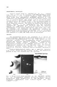
A REVIEW OF SILICON-ON-INSULATOR FORMATION BY OXYGEN ION IMPLANTATION RUSSELL F. PINIZZOTTO Materials Science Laboratory, Texas Instruments Incorporated, P.O.Box 225936, M.S.147, Dallas, Texas, 75265, USA ABSTRACT Silicon-on-Insulator structures will be an important technological advance used in future VLSI, VHSIC and threedimensional integrated circuits. The most mature SOI technology other than silicon-on-sapphire is SIMOX, or Separation by IMplanted OXygen. High energy oxygen ions are implanted into single crystal silicon until a stoichiometric buried silicon dioxide layer is formed. After implantation, the material is annealed at high temperature to remove implantation induced defects. The structure is completed by the growth of a thin epitaxial silicon layer. Devices and complex circuits have been successfully fabricated by several research groups. This paper reviews the development of this buried oxide SOI technology from 1973 to 1983. The five major sections discuss the advantages of SOI, the basics of buried oxide formation, the literature published between 1973 and 1983, key issues that must be solved before large scale implementation takes place and, finally, predictions of future developments. INTRODUCTION This paper is a review of silicon-on-insulator (SOI) formation by oxygen ion implantation. It covers research published in scientific periodicals from 1973 to mid-1983. It is divided into five sections. The first section is a brief overview of the advantages of SOl technology. It explains why SOl may be used in the production of ICs in the near future. The second section presents the basic principles of buried oxide formation. The third section reviews the literature from the classic nitrogen implantation paper of Dexter, Watelski and Picraux J I] to the most recent electric field shielding layer work of Nakashima, Akiya and Kato [2]. The fourth section discusses the issues that will determine whether or not buried oxide SOI is used in production. The last section is the weakest and most controversial. I will make some predictions about future developments and will go on record with specific dates for several major milestones. I hope that these predictions will appear reasonable to those with the enviable position of making postdictions on the same topic. THE Al)VANTAGES OF SO[ The advantages of SOI naturally fall into 4 categories. The first is the improved resistance to radiation induced failures. A typical SOI structure is shown in Figure 1. The devices are physically and electrically separated from one another and from the substrate. Any charge formed in the substrate by ionizing radiation cannot directly affect the active devices because it must pass through the dielectric isolation layer. Only that charge produced in the thin surface silicon film is detrimental. This is a small volume compared to the bulk volume, so SOI circuits should be radiation hard. In addition, soft errors will be minimized and the effects of secondary impact ionization will be reduced.
Mat.
Res. Soc. Symp.
Proc. Vol.
2
Data Loading...