A Study of Defects in Ordered Ternary Semiconductor Epilayers
- PDF / 2,471,205 Bytes
- 6 Pages / 420.48 x 639 pts Page_size
- 3 Downloads / 360 Views
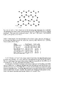
A STUDY OF DEFECTS IN ORDERED TERNARY SEMICONDUCTOR EPILAYERS. S. McKernan, C. B. Carter, D.P.Bour*t, and J.R. Shealy* Department of Materials Science and Engineering, Bard Hall, Cornell University, Ithaca, NY 14853 * School of Electrical Engineering, Phillips Hall, Cornell University, Ithaca, NY 14853 t Present address: David Sarnoff Research Center, Princeton, NJ 08543-5300 ABSTRACT Ordered GaxInl-xP epilayers grown on GaAs substrates have been studied in the electron microscope. Dark-field images and high-resolution micrographs have directly revealed the presence of an ordering of the Ga and In (111) planes. Several different planar defects have been identified in the ordered structure. There is a very high density of faults parallel to the (001) growth surface. Models for these faults have been constructed in terms of stacking faults and twin boundaries in the ordered structure. Other flat planar defects which occur approximately parallel to (111) and (11 i) planes can also be described in these terms. INTRODUCTION The growth of ternary III-V semiconductors by organo-metallic vapor phase epitaxy (OMVPE) is generally assumed to occur such that the structure is the same as that of the binary semiconductors, but with the two different cation or anion species arrayed randomly on their appropriate sublattice sites. Recently electron microscopy studies [1-9] have shown that ordered states exist for several different ternary compounds, and that the properties of the ordered alloy differ from those of the random one. For example, ordered Ga0. 5In05.P grown by OMVPE is characterized 6y a bandgap approximately 50meV less than that of the random alloy. The ordered structure of Ga0 .5 In0 .P 5 is shown schematically in figure 1. The Ga and In forms (111) planes which are Ga rich and In rich alternately. For the present study GaxInl-xP, with x-0.5, was grown on (100) GaAs substrates onto which a 0.5 gtm GaAs buffer layer had been deposited. The growth temperature was 625`C and trimethlygalium (TMGa), trimethylindium (TMIn) and phosphine were used as the sources. The "V:II" flux ratio was approximately 400:1, the growth rate was 35nm/min and the layers were grown to a thickness of approximately 0.5 gtm. These growth conditions produce lattice matched Ga 0 .5In 0 .5 P with a bandgap of 1.84 ev, while material grown at 700"C (which did not show this ordering) had a bandgap of 1.89 ev. Cross-section specimens were prepared for microscopy in the usual manner by cleaving the samples normal to growth surface. Two orthogonal cleaves were epoxied together faceto-face to form the cross section, ensuring that the ordered (111) planes could be observed "endon". The samples were mechanically polished and finally ion thinned to electron transparency with 3 kV Ar+ ions in a liquid nitrogen cooled stage. Plan-view specimens were also prepared by chemical etching to remove the GaAs substrate and buffer layer, followed by Ar+ ion milling to reduce the thickness of the layer to electron transparency. The electron microscopy was performed in a
Data Loading...