Structural Defects in Ion Implanted 4H-SiC Epilayers
- PDF / 6,224,635 Bytes
- 5 Pages / 595 x 842 pts (A4) Page_size
- 45 Downloads / 350 Views
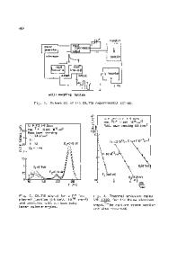
Structural Defects in Ion Implanted 4H-SiC Epilayers P. O. Å. Persson1, W. Skorupa2, D. Panknin2, A. Kuznetsov3, A. Hallén3 and L. Hultman1 1 Thin Film Physics Division, Department of Physics, Linköping University, S-581 83 Linköping, Sweden. 2 FWIM Forschungszentrum Rossendorf, D-01474 Schoenfeld-Weissig, Germany. 3 Royal Institute of Technology, Solid State Electronics, P.O. Box E229, S-164 40 KistaStockholm, Sweden. ABSTRACT Transmission electron microscopy (TEM) was used to investigate Al, Ar, C and Si ionimplanted 4H-SiC epilayers. After the implantation the samples were thermally annealed for 30 minutes at 1700°C. During the annealing process dislocation loops are formed and the generation of such dislocation loops upon annealing, is investigated with respect to dopant electrical activation, peak ion concentration and calculated interstitial/vacancy concentrations. It is concluded that the dislocation loops are generated as the result of a combination of residual damage and excess interstitials generated in a "plus one" (+1) process. INTRODUCTION Silicon carbide (SiC) has over the years gained an interest due to its excellent electrical, chemical and mechanical properties [1,2]. For the purpose of producing SiC-planar devices, selective area doping is needed. Since diffusion of candidate dopant elements in SiC is next to negligible, ion implantation is used to introduce dopants into the material. This technique has other benefits in the sense that it can offer components with tailored doping profiles and concentration. The as-implanted ions predominantly occupy interstitial sites where they are electrically inactive [3], a thermal annealing process is therefore used to position the dopants at substitutional sites, i.e. to activate the dopants. During the implantation process, at doses lower than the apparent amorphisation level, the SiC lattice is still damaged, as Si and C vacancies and interstitials are generated. Cross sectional transmission electron microscopy (XTEM), of these, shows no extended structural defects. During annealing, the crystal is almost completely restored, although, dislocation loops, typically 1-10 nm wide, can form mainly around the mean projected range of the ions. Similar defects have been found in both neutron irradiated and ion implanted cubic SiC polytypes. The investigations so far, however, have not been conclusive with respect to the origin and nature of the defect and it is the intention of this paper to investigate this subject. For this purpose, samples were implanted with Al-, Ar-, C- and Si-ions. After that the samples were subject to annealing and transmission electron microscopy was used to investigate the generated dislocation loops. EXPERIMENTAL The samples were prepared from epitaxially grown 4H SiC layers on (0001) substrates oriented 3.5° off towards (11-20). The layers were implanted with normal incidence by ions at a temperature of 600°C. The implanted samples were annealed at 1700°C for 30 min. The high temperature annealing experiments were performed in a vertic
Data Loading...