A Study of the Performance of an N -Channel MOSFET Under Gamma Radiation as a Dosimeter
- PDF / 2,774,534 Bytes
- 11 Pages / 593.972 x 792 pts Page_size
- 93 Downloads / 268 Views
https://doi.org/10.1007/s11664-020-08330-4 Ó 2020 The Minerals, Metals & Materials Society
A Study of the Performance of an N-Channel MOSFET Under Gamma Radiation as a Dosimeter H.A. FARROH,1,3 A. NASR
,2,4,5 and K.A. SHARSHAR2,6
1.—Radiation Protection and Dosimetry Department, NCRRT, Atomic Energy Authority, Nasr City, Cairo, Egypt. 2.—Radiation Engineering Department, NCRRT, Atomic Energy Authority, Nasr City, Cairo, Egypt. 3.—e-mail: [email protected]. 4.—e-mail: [email protected]. 5.—e-mail: [email protected]. 6.—e-mail: [email protected]
This paper is devoted to the effect of gamma radiation on commercial IRFP250 N-channel metal oxide semiconductor field effect transistors (MOSFETs) in a dose range from 0.5 Gy up to 50 Gy. The device under investigation can be utilized for radiation therapy and dose detection and measurement. The different MOSFETs parameters such as drain current ID, threshold voltage Vth, sensitivity S, transconductance G, and annealing are studied. The main goal of this work is to accurately determine the previous parameters before and after ionizing radiation. From the obtained results, one can estimate the dosage by measuring the mentioned device parameters. The study will be of benefit not only for MOSFET applications as a dosimeter, but also for selecting the type which can tolerate this kind of radiation, especially for space and satellite applications. Finally, the annealing process is done at different temperatures and time. This will aid in determining the ability of the device under test (DUT) to recover. Therefore, the fading of the DUT is studied. From our results, the MOSFET device has excellent properties as a dosimeter. Moreover, in our case, the transconductance and sensitivity were enhanced after irradiation. Key words: Gamma radiation, MOSFET, dosimeter, ionizing radiation effects, 60Co irradiation facility, drain current and gate voltage, sensitivity, transconductance
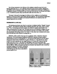
INTRODUCTION Instrumentation used in the field of nuclear and space applications may often be exposed to ionizing radiation of very high intensity. Considerable attention must therefore be given to the possible effects of such an environment on electronic components, and particularly on semiconductor devices, for example, when MOSFETs are irradiated.1–3 Radiation dosimeters include of a variety of devices, such as thermoluminescence crystals (TLDs), ionization chambers, and metal oxide field effect semiconductor transistors (MOSFETs).4–8 The study of radiation effects on MOSFETs,
(Received January 19, 2020; accepted July 11, 2020)
whether n- or p-type, has been an active field of research over recent decades.9 N-Channel MOSFETs, also known as radiation-sensitive field effect transistors (RADFET) or NMOS dosimeters, have been shown to be suitable for dose measurements in various applications including radiotherapy,10–16 space radiation monitoring,17–23 irradiation of food plants,24 and wireless sensors.25 In medicine, radiation is mainly used in diagnostic radiology and radiation oncol
Data Loading...