A study on the importance of isolation of the active regions for high performance organic circuits
- PDF / 263,979 Bytes
- 6 Pages / 432 x 648 pts Page_size
- 31 Downloads / 347 Views
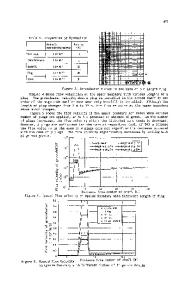
A study on the importance of isolation of the active regions for high performance organic circuits R. Myers, D.Donaghy, M. Raja Organic Electronics Group, Department of Electrical Engineering and Electronics, University of Liverpool, Brownlow Hill, Liverpool, L69 3GJ, UK ABSTRACT The authors present electrical comparisons on an array of test structures including organic lateral diodes and thin film transistors (OTFT), fabricated with a range of disordered and polycrystalline organic semiconductors, to examine the increasing need for effective isolation for organic-based circuits. As the minimum feature size decreases, circuit components become closely positioned, which leads to increased electrical crosstalk. The organic semiconductors utilised for this work include solution-processable organic semiconductors such as disordered polymers P3HT and PTAA, and a polycrystalline material TIPS-pentacene. In order to predict the magnitude required for isolation for the different semiconductors, simple test structures have been designed consisting of two gold electrodes separated by a distance ranging from 4 μm up to 2000 μm. The bulk conductivity from such test structures provides the limits at which circuit components may be placed for crosstalk free operation. The work presented culminates in the development of an isolation layer to help reduce the off-currents and gate leakages of the OTFTs. INTRODUCTION The continuous improvement made to organic semiconductor materials (both disordered and polycrystalline) over recent years have resulted in significant enhancements in electrical performance and field effect mobilities [1]. As this rate of advancement is maintained the possibilities for the development of multi-component functional organic circuitry increase greatly. For example, one direct effect on OTFTs is the reduction of device dimensions as large channel widths are no longer required to obtain comparable on-currents and field effect mobilities, as is the case with lower performing materials. This leads to the opportunity to produce organic circuits with more devices per unit area with more complicated designs. Another instigator for more compact organic circuits is the reduction of the minimum feature size, as this decreases, devices can be positioned much more closely together. This results in a significant increased electrical crosstalk between circuit components and functional blocks, especially with organic semiconductors with no isolation technique applied. This introduces capacitive, inductive or conductive coupling as well as increased gate leakages, these can slow down a circuits’ speed of operation severely. Numerous methods of patterning or isolation of the organic semiconductor active area have been applied; including laser ablation [2], subtractive and additive photolithography [3], selective surface energy engineering [4], ink jet printing [5] and thermal evaporation through a shadow mask [6]. Some of these methods are directly applied after the active area is deposited; raising questions on how the or
Data Loading...