A1 2 O 3 as a Transition Layer for GaN and InGaN growth on ZnO by MOCVD
- PDF / 229,118 Bytes
- 6 Pages / 595.22 x 842 pts (A4) Page_size
- 45 Downloads / 294 Views
1201-H06-02
Al2O3 as a Transition Layer for GaN and InGaN growth on ZnO by MOCVD Nola Li1, Shen-Jie Wang1, Will Fenwick1, Andrew Melton1, Chung-Lung Huang2, Zhe Chuan Feng2, Christopher Summers3, Muhammad Jamil1, and Ian Ferguson4 1
Electrical and Computer Engineering, Georgia Institute of Technology, Atlanta, GA 30332
2
Graduate Institute of Photonics and Optoelectronics, and Department of Electrical Engineering,
National Taiwan University, Taipei, Taiwan 106-17, ROC 3
Materials Science and Engineering, Georgia Institute of Technology, Atlanta, GA 30332
4
Electrical and Computer Engineering, University of North Carolina Charlotte, Charlotte, North
Carolina, 28223-0001
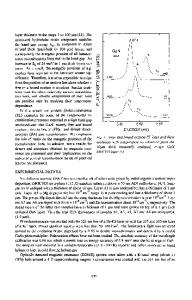
ABSTRACT GaN and InGaN layers were grown on annealed 20 and 50nm Al2O3/ZnO substrates by metalorganic chemical vapor deposition (MOCVD). GaN was only observed by high resolution x-ray diffraction (HRXRD) on 20 nm Al2O3/ZnO substrates. Room temperature photoluminescence (RT-PL) showed the red shift of the GaN near band-edge emission, which might be from oxygen incorporation forming a shallow donor-related level in GaN. HRXRD measurements revealed that (0002) InGaN layers were also successfully grown on 20nm Al2O3/ZnO substrates. In addition, thick InGaN layers (~200-300nm) were successfully grown on Al2O3/ZnO and bare ZnO substrates. These results are significant as previous studies showed decomposition of the layer at InGaN thicknesses of 100nm or less.
INTRODUCTION ZnO is an ideal substrate for epitaxial growth of GaN and InGaN. ZnO has the same wurtzite structure as GaN with a small c-plane lattice mismatch of only 1.8% [1,2]. It offers structural similarities to GaN over the non-native substrate materials, such as sapphire and SiC, which have large mismatches in lattice constant. InGaN, with a composition of 18% indium, has a perfect lattice-match with ZnO in the a-axis direction, which allows for the possible growth of InGaN layers without misfit dislocations [1-3]. Furthermore, ZnO and GaN have a similar thermal expansion coefficient which allows for almost zero thermal strain [4]. ZnO is a conductive material allowing it to be utilized in vertical structures to form electrodes on both sides. It is also easily etched chemically allowing for a thin GaN structure [5]. Metalorganic chemical vapor deposition (MOCVD) is the most widely used epitaxial growth method in industry; and therefore, studies in this report will be done by MOCVD. MOCVD growth is performed at high temperatures where ZnO substrates decompose causing diffusion of Zn and O into the epilayers. NH3, as the nitrogen precursor, decomposes at a high temperature contributing H2 to the atmosphere, which back etches the ZnO surface forming etched pits and
surface peel off [6]. Previously, dimethylhydrazine (DMHy) was used as a nitrogen source for the GaN growth on sapphire due to higher cracking efficiency at low temperature (420°C) compared with NH3 (15% decomposes at 950oC) [7, 8]. More recently, a ZnO film was investigated as a buffer layer for GaN growth on sapphire by MOC
Data Loading...