High Resolution X-ray Diffraction and X-ray Topography Study of Gan on A1 2 O 3
- PDF / 1,150,574 Bytes
- 6 Pages / 414.72 x 648 pts Page_size
- 47 Downloads / 206 Views
2.75 gm except sample number six. The thickness of the GaN filmin samplenumber six is 2.0 pm. The optical photomicrograph ofthe sample numberthree whichhas no bufferlayer show atypical hexagonal morphology as expected from a GaN filmwithout any buffer layer. The photomicrographs of all the othersamples showed a optically smooth surface as expected from a good quality epitaxial GaN film. Table I: Description of the GaN/A120 3 samples. Sample No.
I& 2
3 4 5
6
Description
Growth Temp. Mobility
Grown with a thinner AIN buffer layer. Sample no. I and 2 comes from the edge and center part of the sample, respectively. Remarkable differences in mobility was found in these two samples. Grown without a buffer layer. Grown with a GaN buffer layer. Grown with an AIN buffer layer, This sample is highly resistive but was Grown at a time when similar samples were doped with Si to a carrier conc. of 6.OxlIO 6 and mobility 500 cm2/V.s. Grown with an AIN buffer layer and at a slightly lower temperature, highly resistive.
2
Carrier
(OC)
cm /V.s
1035
347
1.4x10 17
44
1.0xl017
310 548
7.Oxl017 6.Oxl016
1039.5 1037.5 1035
Conc.
1020
Table II: Extinction length and structure factors in GaN using CuKch radiation for selected symmetric and asymmetric reflections. Reflection 00.2 00.4 00.6 01.4 01.5 11.4 02.4 02.5
Extinction Length (4•m)
Structure Factor Frh
FPh
0.449 2.011 12.0 5.360 7.298 2.827 12.08 20.011
47.705 29,690 24.210 6.263 22.041 24.264 6.407 19.686
-7.854 1.518 5.094 12.366 -13.87 1.518 -9.579 10.504
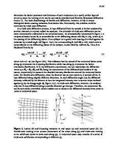
Lattice parameters and structure of the GaN thin films were obtained using a combination of one symmetric and anumber of asymmetric reflections and were calculated using the following method. 6 IfAOB1 and AOB2 are the angular differences between the epilayer and substrate rocking curve peak positions at 00 and 1800 azimuthal rotation, respectively, then the Bragg angle difference between the epilayerand substrate lattices, AOB, is given by A0B = (A0O1 + AO, 2)/2, and the misorientation between the substrate and epilayer lattices is given as (AOBI -Ae, 2)/2. In selecting a reflection one must be careful that the thickness of the film should not be smaller than the extinction length. The extinction length, l,, for a wavelengthXis given by the relation 316
1=-
(1)
where yO=sin(OB-q) and yh=sin(0 5+n) are the direction cosines of the incident and diffracted waves, respectively, 0 , is the Bragg angle of diffraction, anda is the angle between the crystal surface and reflection plane. The polarization factorC is the unity fora polarization and cos(20B)forx polarization. The quantities )("h=r X•Frh x - reF h-
(2)
are the hth Fourier coefficients ofthe polarizability multiplied by 4n, r, is the classical electron radius, V isthe unit-cell volume, and Fh, FPh are the real and imaginary parts of the structure factor. Structures factors were calculated by using reference. ITable II summarizes the structures factors, and the extinction length in GaN using CuKa, radiation for several symmetric and asymmetric r
Data Loading...