AFM Induced Local Oxidation of HOPG
- PDF / 587,483 Bytes
- 5 Pages / 612 x 792 pts (letter) Page_size
- 11 Downloads / 267 Views
AFM Induced Local Oxidation of HOPG Kenichi Uki, Mikihiro Kato, Susumu Harako, Xinwei Zhao Advanced Device Laboratories and Department of Physics, Tokyo University of Science. Shinjuku, Tokyo 162-8601, Japan Phone: +81-3-3260-4272 E-mail: [email protected] ABSTRACT AFM induced local anodic oxidation of HOPG was carried out in various conditions such as humidity, applied voltage and scan speed. A clear evidence of different oxidation features between HOPG and graphene has been confirmed and discussed. These results should contribute to the progress of the micro/nano fabrication of graphene by the local anodic oxidation.
INTRODUCTION Graphene has many excellent properties, such as high electric mobility, transparency and high thermostability[1-11]. Thus, it has been attracting attention for the next generation electronic devices. The graphene made by scotch tape method is widely used for studying its physical properties. This method puts scotch tape on HOPG (Highly Ordered Pyrolytic Graphite), then peels off a sheet and transfers the sheet to a substrate. Therefore, nanofabrication of graphene by AFM (Atomic Force Microscope) induced local anodic oxidation becomes available, which may expand the applications of graphene to nano electric devices. There have been some works on, anodic oxidation of graphene by AFM[12-15]. However, most of these experiments were carried out in high humidity, which resulted in a low practicality. Furthermore, some sample’s surface is raised after the oxidation, and other sample’s surface is depressed. The unified theory has not been accomplished yet. In this work, we carried out the AFM oxidation of HOPG in various humidity, in order to find a suitable process of nanofabrication using graphene. Different oxidation features of raising or depressing the sample surface, by changing thickness of HOPG, have been confirmed. METHOD First, a SiO2 layer (~ 300 nm) was formed on Si substrate by baking the Si in a muffle furnace for 10 hours at 1000oC. Next, HOPG was peeled by using scotch tape for 10 times, and then transfered to the SiO2 surface. Afterwards, Au(100nm)/Ni(5nm) electrodes were formed by photolithography and vacuum deposition on parts of the graphene areas.
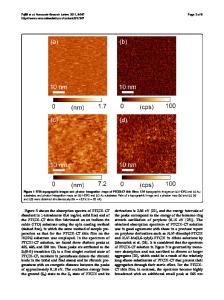
RESULTS AND DISCUSSION We have oxidized thick samples (HOPG thickness of 80nm) and thin samples (40nm), and obtained different results. The thick graphene samples exhibited subsidence surfaces. In contrast, the thin samples showed raised surfaces. Sample of subsidence surface The anodic oxidation of the thick samples was carried out by applying bias voltages on the AFM cantilever in changing humidity, applied voltage and scan speed.
[a] Relative humidity 45[%]
[b] Relative humidity 40[%]
[c] Relative humidity 30[%]
Fig.1. AFM Images of after local anodic oxidation in change humidity.
[a] Relation of height and scan speed at 7 V
[b] Relation of width and scan speed at 6 V
Fig.2. Relation of scan speed with depth and width of the holes.
[a] Relation of height and voltage
[b] Relation of width and voltage
Fig.3. R
Data Loading...