Afm Study of Surface Morphology of High Dose Co Implanted Si with A Mevva Ion Source
- PDF / 2,112,601 Bytes
- 6 Pages / 414.72 x 648 pts Page_size
- 28 Downloads / 318 Views
shown the ability to form buried epitaxial CoSi 2 layers in silicon with good crystal quality and good electrical properties [3-10]. In particular, the formation of CoSi2 layers in Si by implantation with a metal vapor vacuum arc (MEVVA) ion source, a new type of ion source operating in pulse mode and having broad beam and high beam current capability, has recently been achieved [11,12]. However, there is little work reported on the study of the surface morphology of Co implanted Si samples. In this paper, we shall present some of our preliminary results on the application of atomic force microscopy (AFM) to studying the surface morphology of Co implanted Si with a MEVVA ion source. EXPERIMENTAL High dose Co implantation into Si was performed using a MEVVA ion source at an extraction voltage of 60 or 70 kV to a dose of 2x10 17 or 4A10 17 ions cm- 2 . The silicon substrates used were (100) p-type with a resistivity of 10-20 Q2cm or 0.01-0.02 Qcm. The substrate was subjected to severe beam heating because of the high beam current of the MEVVA source. The average substrate temperature Ts during implantation was adjusted by varying the beam current and was measured by a thermocouple. An AFM was used to observe the surface morphology of the implanted samples. AFM images were taken in 763 Mat. Res. Soc. Symp. Proc. Vol. 396 01996 Materials Research Society
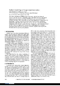
ambient air and the images were acquired in the constant force mode using a standard AFM cantilever. The loading force was set as 10-8 N. RESULTS Typical AFM images of the (100) p-Si wafers of 10-20 f•cm implanted at 70 kV and a dose of 2x10 17 ions cm- 2 at substrate temperatures of 210 0 C, 4000 C, 4600C and 7000 C are shown in Figs. 1 to 4, respectively. The AFM image of the (100) p-Si substrate of 0.01-0.02 f2cm implanted at a voltage of 60 kV and a dose of 2x10 17 ions cm- 2 at Ts of 3000 C is shown in Fig. 5. A plot of the root-mean-square roughness determined from AFM measurements versus Ts is given in Fig. 6. From Fig. 6, Rrms is seen to span a large range from subnanometer scale for the sample with Ts of 2100C to about 35 nm for the sample with Ts of 7000 C. It is also observed that Rrms increases with Ts exponentially for Ts less than about 6000C when other parameters are fixed. The relation as indicated by the dotted straight line is given by RrIs (Ts) = Ro exp (TsITo) where Ts is in K and Ro and To are determined to be about 0.12 nm and 250K, respectively.
DISCUSSION From Figs. 1 to 5, we can see that when Ts is less than about 600 0 C, the surface morphology of the implanted samples shows largely similar features of densely distributed small sized asperities. However, for the sample with Ts of 7000 C, the surface morphology is seen to be significantly different and shows hillocks of much larger size. The occurrence of such a dramatic change in morphology near 7000 C is believed to be related to the fact that a substrate temperature of about 600-700 0 C is required for significant growth of CoSi 2 . From Fig. 6, the exponential dependence of surface roug
Data Loading...