AFM Analysis Of Nano-Copper Surface Morphology
- PDF / 1,373,523 Bytes
- 6 Pages / 612 x 792 pts (letter) Page_size
- 36 Downloads / 402 Views
BB5.3.1
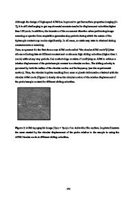
AFM Analysis Of Nano-Copper Surface Morphology. Rynno Lohmus**, Irina Hussainova*, Lembit Kommel*, Hele Siimon** * Department of Materials Engineering, Tallinn University of Technology Ehitajate tee 5, 19086 Tallinn, Estonia ** Institute of Physics, University of Tartu, Riia 142, 51014 Tartu, Estonia Abstract. Surface morphology and features of pure copper heavily deformed by equal channel angular pressing were studied by means of an atomic force microscope (AFM) and scanning electron microscope (SEM) techniques. Surface characterization helps to develop a better understanding of microstructure evolution of materials subjected to any kind of mechanical loading and thermal treatment. The main objectives of this study are to exploit the capabilities of AFM to accurately perform an analysis of the surface features of nano-structured copper subjected to plastic deformation and heat treatment; and examination of the mechanical characteristics influenced by material’s microstructure. It is shown that the AFM technique can be extremely useful for the investigations of a surface topography of materials. Keywords: Atomic Force Microscopy; Nanostructure; Severe Plastic Deformation; Grain Boundary 1. Introduction With the emergence of nanotechnology and nanoscience the investigation and application of nanostructured materials is growing rapidly. By definition, these materials have at least one dimension that is less than 200 nanometers. As the fabrication of novel materials and miniaturisized devices continues to progress at breakneck speed, the need for new test techniques commensurate with much smaller dimension has become even more evident within the research community. The AFM is ideally suited for both visualization of nanostructured materials and for measuring the spatial dimensions of features at the surface. Atomic Force Microscopy is a form of scanning probe microscopy where a small probe is scanned across the sample to obtain information about the sample's surface. Interatomic forces between the probe tip and the sample surface cause the cantilever to deflect as the sample's surface topography (or other properties) changes. A laser light reflected from the back of the cantilever measures the force via deflection of the cantilever, and this information has feed back to a computer, which generates a map of topography and/or simultaneouslyother properties of interest. Due to high resolution AFM can be used for studying the surface features of various materials [1, 2]. Nanostructural materials often exhibit unique mechanical properties that make them a subject of intensive fundamental research [2 - 5]. Nanocrystalline metals have strengths exceeding those of coarse-grained and even alloyed metals, however, often exhibit low tensile ductility at room temperature, which limits their practical utility. In contrast to many nanocrystalline materials, nanostructured copper possesses both high strength and plasticity as a result of appropriate heat treatment. At the same time, available reported data [6 - 9] show a sig
Data Loading...