AlGaN Transition Layers on Si (111) Substrates - Observations of Microstructure and Impact on Material Quality
- PDF / 1,805,450 Bytes
- 6 Pages / 612 x 792 pts (letter) Page_size
- 30 Downloads / 346 Views
1068-C06-03
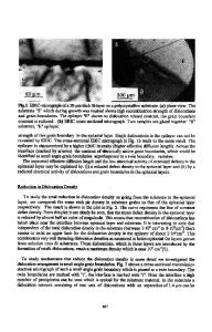
AlGaN Transition Layers on Si (111) Substrates - Observations of Microstructure and Impact on Material Quality John C. Roberts, James W. Cook, Jr., Pradeep Rajagopal, Edwin L. Piner, and Kevin J. Linthicum Nitronex Corporation, 2305 Presidential Drive, Durham, NC, 27703 ABSTRACT AlGaN based transition layers are one proven solution used for the growth of device quality GaN layers on Si(111) substrates. Examination of the microstructure of GaN on silicon epitaxy grown with these AlGaN transition layers, by transmission electron microscopy (TEM) and other methods, reveals some interesting properties that can help explain how high quality IIIN epitaxy can be performed in a system with significant thermal and lattice mismatch. The existence of a thin amorphous SiNx layer at the silicon substrate/transition layer interface has been documented. This amorphous SiNx layer accommodates stress at this interface as well as affecting a reduction of the formation of misfit dislocations. Relatively low screw dislocation densities (less than ~107 cm-2) are also observed in GaN on silicon films grown with AlGaN based transition layers. These microstructural characteristics contribute to the overall high quality of the AlGaN/GaN HEMT epitaxial structures that are grown on Si(111) substrates utilizing AlGaN transition layers. INTRODUCTION AlGaN/GaN based high electron mobility transistors (HEMTs) have emerged from the realm of research and development and are being evaluated and designed into systems in the commercial and military sectors that require high power and high efficiency amplification with excellent linearity and/or bandwidth. To date, the vast majority of devices being considered for such systems are based on some type of heteroepitaxial growth, due to the lack of a commercially available GaN substrate that is cost effective and readily available in suitable quantities. The most common substrates used for high power AlGaN/GaN based devices are silicon carbide, silicon, and sapphire, each of which has specific advantages and disadvantages. Silicon has numerous advantages as a substrate choice for III-N heteroepitaxy. It is an extremely mature substrate technology, where wafers 100 mm in diameter and larger are readily available from a multiplicity of vendors for a few tens of dollars per wafer. Due to the maturity of the silicon wafer industry, substrate quality is extremely high, and wafer to wafer consistency is superb. The availability of very large diameter silicon substrates currently enables the GaN on silicon approach as the only platform with an immediate roadmap to wafer sizes 150 mm in diameter and beyond. From a manufacturing standpoint, choosing silicon as the substrate also leverages the capability to use existing high volume silicon process services and assembly houses (e.g., wafer thinning, via technology, dicing, and plastic over-mold packaging). There are also challenges associated with using silicon as the substrate for III-N materials. Growth of high quality GaN on Si(111) can be achieved on
Data Loading...