Molecular Beam Epitaxy of AlN Layers on Si (111)
- PDF / 222,475 Bytes
- 5 Pages / 595 x 842 pts (A4) Page_size
- 3 Downloads / 368 Views
1068-C03-05
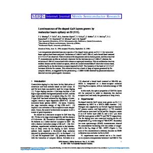
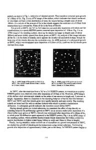
Molecular Beam Epitaxy of AlN Layers on Si (111) Jean-Christophe Moreno, Eric Frayssinet, Fabrice Semond, and Jean Massies CRHEA-CNRS, rue Bernard Gregory, Valbonne, 06560, France ABSTRACT In this work, aluminum nitride (AlN) thin films are epitaxially grown by Molecular Beam Epitaxy (MBE) on silicon substrates in order to fabricate thin film bulk acoustic resonators (TFBARs). Using atomic force microscopy, scanning electron microscopy and Xray diffraction, we study the quality of AlN films as a function of different silicon surface preparation techniques. Finally, acoustic picosecond measurements are presented. INTRODUCTION In recent years, AlN thin films have attracted much attention for optoelectronic and acoustic applications [1-4]. AlN is potentially a very interesting material because it is a highband gap piezoelectric semiconductor material having a high cohesive energy and furthermore it is compatible with the silicon technology. Present AlN-based FBAR filters are fabricated with AlN films that are deposited by sputtering [5, 6]. Although sputtered AlN films are polycrystalline, films having a thickness above 1 μm are sufficiently well oriented that the piezoelectric coupling (Kt2) is close to the value expected for bulk single crystals. Nowadays the wireless telecommunications development needs to handle higher frequencies where submicron AlN films would be required. However, the degradation of the quality of submicron AlN films deposited by sputtering as well as the related increases of insertion losses is reported and seems to be a limiting factor to further increases operating frequencies. On the other hand epitaxial AlN thin films are expected to behave like bulk single crystals and their quality is not expected to depend a lot with the film thickness. During the last 10 years, an efficient growth process has been developed at CRHEA about the epitaxy of group III-nitride on silicon substrates [7]. Although mainly dedicated to the fabrication of GaN-based transistor devices, this has resulted in the ability to grow smooth epitaxial AlN films on silicon substrates. So, we propose to use epitaxial AlN thin films grown on silicon substrates to realize advanced high frequency bulk acoustic wave devices for filtering and time reference (oscillators) applications. EXPERIMENT AlN epitaxial films are grown on 2” silicon (111) wafers. Obviously in the silicon technology, the (111) surface orientation is much less used than the (100) but it turns out that the hexagonal surface symmetry of (111) orientation is more appropriate to grow the AlN wurtzite phase. Also, using such surface orientation only one AlN polarity is grown, actually only the Al-polarity can be grown, and no inversion domains are usually observed. Three different silicon surface preparation techniques are assessed in this work. The first one consists in an ex-situ standard chemical cleaning followed by an H-passivation using a diluted HF solution with a subsequent de-ionized water rinsing [8, 9]. Then wafers are loaded in the MBE grow
Data Loading...