Growth of aligned multiwalled carbon nanotubes on bulk copper substrates by chemical vapor deposition
- PDF / 1,394,915 Bytes
- 8 Pages / 584.957 x 782.986 pts Page_size
- 60 Downloads / 454 Views
Mark Schulz Department of Mechanical Engineering, University of Cincinnati, Cincinnati, Ohio 45221-0072
Vesselin Shanova) Department of Chemical and Materials Engineering, University of Cincinnati, Cincinnati, Ohio 45221-0012 (Received 24 March 2009; accepted 18 April 2009)
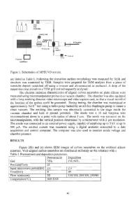
Successful growth of vertically aligned carbon nanotube (CNT) arrays on copper substrate by thermal chemical vapor deposition is reported in this paper. The effects of Ti, Ni, and Ni–Cr intermediate layers have been studied to eliminate cracking of the copper surface during the synthesis of CNTs. It was found that these intermediate layers play a critical role in achieving vertical alignment of CNTs on copper substrates. The effects of other reaction parameters such as flow rate of ethylene, concentration of water vapor, and deposition temperature have also been studied. Scanning electron microscopy, transmission electron microscopy, and micro-Raman spectroscopy were used to evaluate the quality and nature of the CNT formed. I. INTRODUCTION
High-power consumption and heat dissipation are two of the most serious limitations in today’s highperformance electronics. The superior thermal conductivity of carbon nanotubes (CNTs) has prompted suggestions of their applications in thermal management of high-power electronics.1 Since the discovery of CNTs in the early 1990s, they have gathered much interest because of their unique electrical, mechanical, and electronic properties for fabrication of nanometer-scale devices. It is expected that, in thermal management applications, the performance of the integrated circuits (IC) can be dramatically improved by using conducting metal substrates with CNTs directly synthesized on them.2 In recent years, there has been a considerable increase in the development of new strategies for creating CNT structures directly attached to conducting substrates. One approach is to transfer CNT arrays from Si substrates onto conducting substrates.1,3,4 In this method, several intermediate steps were associated with preparing adhesive coating. Beside, the CNTs are usually distributed uniformly and do not adhere properly to the surface of the substrates. These problems can be overcome by the second approach that is directly synthesizing CNTs on conducting substrates. Furthermore, the mechanical properties will also be greatly enhanced with low-contact
a)
Address all correspondence to this author. e-mail: [email protected] DOI: 10.1557/JMR.2009.0339 J. Mater. Res., Vol. 24, No. 9, Sep 2009
http://journals.cambridge.org
Downloaded: 01 Apr 2015
resistance between the CNTs and the conducting substrates. With higher electrical conductivity, better electromigration resistance, and superior trench-filling capability, copper has replaced aluminum alloys in on-chip metallization metal for interconnection and also dominates in applications for printed circuit boards (PCBs).5 Earlier studies related to synthesis of CNTs on bulk stainless steel and Inconel substrates by plasma-enhanced chemical vapor deposition (PECVD) have bee
Data Loading...