Analysis of Teos Silicon Dioxide: The Identification of Carbonatious Contaminants
- PDF / 265,901 Bytes
- 4 Pages / 414.72 x 648 pts Page_size
- 78 Downloads / 282 Views
precursors, the resultant ratio of C / Si = 0.01% (about 100 ppm). So the task is clear, to characterize the deposited films and try to identify the carbonatious residues. EXPERIMENTAL RESULTS
The silicon dioxide films were deposited from the reaction of Si(TEO) 4 + 02 on a home built multichambered PECVD system. The silicon substrates were (100), p-type, 10-20 Q-cm, and the deposition parameters, pressure = 1.5 Torr, RF power = 200 W, temperature of 360 0 C, electrode - substrate distance of 1.5 cm , and volumetric flow rates of 02 and TEOS of 100 and 40 sccm respectively. The initial characterization showed an oxide thickness of 0.125 microns, an ellipsometrically obtained index of refraction with a value of 1.434, and a IR spectra with the characteristic bands for Si-O, and Si - OH stretching modes. No evidence of carbon contamination within the detectivity limits of the instrument. Previous Experiments While attempting to perform C-V and I-V measurements on MOSCAP structures using the deposited oxide as the dielectric layer we noticed the formation of bubbles under the aluminum gates upon biasing the MOSCAP. We wanted to be certain that the gas originating from the biasing was the result of a chemical reaction we performed some simple experiments. Detail description of the I-V characteristics are presented in a companion article [4]. By applying positive voltage steps to the gates we could accelerate the formation of the gas 1. bubbles, suggesting a field dependence for the gas release. 97 Mat. Res. Soc. Symp. Proc. Vol. 500 ©1998 Materials Research Society
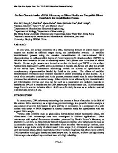
2. When we ramped the voltage, less gas was released, perhaps an indication of enhanced diffusion. 3. We never observed molten aluminum, so local heating and metal evaporation was not the origin of the gas. 4. A sample was heated to 200 0 C for 15 min to outgass, later, it was subjected to a voltage bias and a bubble was formed, eliminating the possibility of desorption as the origin of the gas. 5. The moderate frequency C-V characteristics show a time dependence for the appearance of the first bubble (see figure 1). 400 W 00
Hysteresis(V)
2
~
'A
AI
200 W
-
01 0
20
40 - -
60
8"0
100
1"20
FIRST BUBBLE NOTICED(s) Figure 1.Extent of Hysteresis vs time for occurrence of the first noticeable bubble on the Al gate. The above facts suggest an electrochemical reaction as the possible origin of the bubbles and the gas causing their formation. At this time we decided to divide the characterization effort in two parts, one effort to elucidate the nature of the gas phase, and a second one for the solid phase. Analysis of the Solid Phase We utilized SEM pictures to seek evidence of heterogeneity's which may spatially correlate with the formation of bubbles. No evidence was found to the magnification limit of the instrument. We decided next on SIMS for its low detection limit, we used a beam of O2+, at 13 KeV on a sample with a 150 nm Al gate. The mass spectra was mostly what we expected, except for a high value of C+ (m/z=12) which points to a carbon co
Data Loading...