Analytical Modeling of Triple-Metal Hetero-Dielectric DG SON TFET
- PDF / 1,028,225 Bytes
- 8 Pages / 593.972 x 792 pts Page_size
- 85 Downloads / 346 Views
ÓASM International 1059-9495/$19.00
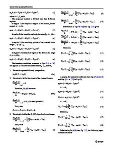
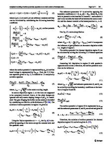
Analytical Modeling of Triple-Metal Hetero-Dielectric DG SON TFET Aman Mahajan, Dinesh Kumar Dash, Pritha Banerjee, and SubirKumar Sarkar (Submitted April 20, 2017; in revised form August 29, 2017) In this paper, a 2-D analytical model of triple-metal hetero-dielectric DG TFET is presented by combining the concepts of triple material gate engineering and hetero-dielectric engineering. Three metals with different work functions are used as both front- and back gate electrodes to modulate the barrier at source/ channel and channel/drain interface. In addition to this, front gate dielectric consists of high-K HfO2 at source end and low-K SiO2 at drain side, whereas back gate dielectric is replaced by air to further improve the ON current of the device. Surface potential and electric field of the proposed device are formulated solving 2-D PoissonÕs equation and YoungÕs approximation. Based on this electric field expression, tunneling current is obtained by using KaneÕs model. Several device parameters are varied to examine the behavior of the proposed device. The analytical model is validated with TCAD simulation results for proving the accuracy of our proposed model. Keywords
ambipolar conduction, analytical model, band-to-band tunneling, TM-HD DG SON TFET, work function engineering
1. Introduction With the advancement in science and technology, there is a gradual reduction in device dimension in order to achieve high speed of operation, reduction in power consumption but miniaturization of transistor leads to various short-channel effects like drain-induced barrier lowering (DIBL), threshold voltage roll-off (TVRO), hot carrier effect (HCE), etc. In order to alleviate such problems, tunnel field effect transistor (TFET)is introduced which works on the principle of bandto-band tunneling (BTBT) instead of thermionic emission as in case of MOSFET and has widespread low power applications (Ref 1). According to the report of IMEC-2010, TFET is the most favorable device which can replace MOSFET in fabrication of VLSI chips (Ref 2). Moreover, steep subthreshold slope of TFET of < 60 mV/decade, higher immunity to SCEs (due to the presence of tunneling barrier), and low OFF current make TFET a possible alternative device in nanometer regime (Ref 35). Apart from these advantages, TFET suffers from limitations of ambipolar conduction and small ON current. In order to overcome these drawbacks, we need to partially or fully modify our device geometry to get higher ON current (Ref 6-9). Dual material gate structure (Ref 9) and gate-on-drain overlap structure (Ref 10) are used to suppress the ambipolar current. Single-material gate hetero-dielectric TFET was introduced with high-K dielectric at source end producing high tunneling current and a low-K dielectric at the drain end suppressing Aman Mahajan, Dinesh Kumar Dash, Pritha Banerjee, and Subir Kumar Sarkar, Department of Electronics and Telecommunication Engineering, Jadavpur University, 188, Raja S. C. Mallick Road, Kolkata 700032, India. Co
Data Loading...


